Effects of As Doping on Properties of ZnO Films
- PDF / 410,285 Bytes
- 6 Pages / 612 x 792 pts (letter) Page_size
- 47 Downloads / 460 Views
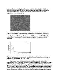
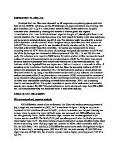
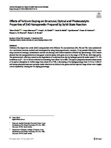
Effects of As Doping on Properties of ZnO Films K.S. Huh, D.K. Hwang, K.H. Bang, M.K. Hong, D. H. Lee, J.M. Myoung Information & Electronic Material Research Laboratory, Department of Materials Science and Engineering, Yonsei University, Seoul 120-749, Korea M.S. Oh, W. K. Choi Thin Film Technology Research Center, Korea Institute of Science and Technology, Seoul 130650, Korea ABSTRACT A series of ZnO thin films with various deposition temperatures were prepared on (100) GaAs substrates by radio-frequency magnetron sputtering using ZnO target. The ZnO films were studied by field emission scanning electron microscope(FESEM), x-ray diffraction(XRD), photoluminescence(PL), cathodoluminescence(CL), and Hall measurements. The structural, optical, and electrical properties of the films were discussed as a function of the deposition temperature. With increasing temperature, the compressive stress in the films was released and their crystalline and optical properties were improved. From the depth profile of As measured by secondary ion mass spectrometry(SIMS), As doping was confirmed, and, in order to activate As dopant atoms, post-annealing treatment was performed. After annealing treatment, electrical and optical properties of the films were changed. INTRODUCTION Recently, zinc oxide (ZnO) has been emerged as an attractive material for application to the optical devices such as blue-, violet-, and UV-light emitting diodes(LEDs) and laser diodes(LDs) [1]. ZnO has very strong spontaneous emissions from bound excitons even at room temperature due to the large exciton binding energy of ~60 meV, as well as has structural and optical properties similar to GaN widely used to optical devices in present. Also, ZnO has high cohesive energy and melting temperature due to the high Zn-O bond strength, resulting in high-temperature stability during process [2,3]. For development of optical devices based on ZnO, GaAs can be used as a useful substrate material and it is attributed to the possibility of high level of monolithic system through the integration of optical components[4]. In addition, GaAs can be used as a p-type dopant source in ZnO film, which is essential to application of ZnO for optoelectronic devices [5]. However, because of the problems related to thermal stability and stress due to large lattice mismatch of about 19 % between ZnO and GaAs, a few studies of ZnO thin film on GaAs have been reported [6-9]. In general, it has known that thin films composed of polycrystalline structures are difficult to apply for optical devices due to the poor optical property originated from defectrelated deep-level emissions[10]. In this study, we report on the effects of deposition temperature on properties of ZnO thin films prepared on GaAs (100) by rf magnetron sputtering. Then, effects of post-annealing treatment for ZnO films were discussed through Hall and PL measurements. EXPERIMENTAL DETAILS ZnO films were deposited by radio frequency(rf) magnetron sputtering. A 2-in. diameter H11.8.1
and 5-N purity ZnO target were used to depo
Data Loading...