Effects of Surface Preparation on Epitaxial GaN on 6H-SiC Deposited Via MOCVD
- PDF / 127,597 Bytes
- 6 Pages / 612 x 792 pts (letter) Page_size
- 41 Downloads / 259 Views
Department of Chemical Engineering, Kansas State University, Manhattan, KS 66506 Department of Mechanical Engineering, Wichita State University, Wichita, KS 67208
**
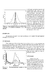
Cite this article as: MRS Internet J. Nitride Semicond. Res. 4S1, G3.39(1999) ABSTRACT A comparison was made of 6H-SiC surfaces etched with H2, C2H4/H2, and HCl/H2, and the resulting crystal quality of epitaxial GaN films deposited on these substrates. To remove the many fine scratches and to smooth the rough surfaces typical of commercial SiC substrates, the Si-face 6H-SiC substrates were etched in H2, C2H4/H2, and HCl/H2 at 1450 oC. GaN was subsequently deposited on these etched surfaces after first depositing a low temperature GaN buffer layer via metalorganic chemical vapor deposition (MOCVD). The surface morphologies after etching and after GaN deposition were characterized by atomic force microscopy and Normaski differential interference contrast microscopy, while the crystal quality of the GaN films was assessed by double crystal x-ray rocking curves and x-ray topography. 6H-SiC substrate surfaces were improved in terms of the removal of scratches and the reduction of surface roughness, and both surface morphology and crystal quality of the subsequently deposited GaN films were enhanced. However, the dislocation density was not decreased by the surface etching. The best GaN film was produced by etching the substrate in pure H2 for 40 minutes before growth. Recommendations for the optimum substrate treatment are made. INTRODUCTION GaN has long been a promising material for optoelectronic devices operating in the blue to ultra-violet region [1-2], but the lack of GaN bulk crystals hinders the improvement of GaN epitaxial film quality. Sapphire is the most common substrate for GaN epitaxy, but because of large differences in lattice constants(13.8%) and thermal expansion coefficients(25.4%), the threading dislocation density is typically high in the GaN film. In contrast, 6H-SiC has a smaller lattice mismatch (3.5%) with GaN, making it a better candidate for GaN growth [3]. High quality GaN was successfully deposited on 6H-SiC substrates via MOCVD by several groups [4-6], but no detailed investigation of the effects of the 6H-SiC substrate surface treatment prior to GaN growth has been reported. Compared to sapphire, the surface quality of commercial 6H-SiC substrates is poor, containing various defects that may deteriorate the quality of epitaxial layer. Some defects, such as dislocations, and micropipes (holes approximately a micrometer in diameter) originate in the bulk of the substrate, while other defects such as ridges and scratches result from the lapping and polishing process. The later defects can be almost fully removed by etching the surface with hydrogen, with or without propane or HCl [7-8]. In the case of SiC epitaxy, defects in the film propagating from the substrate are minimized by in situ etching of substrates [7-8]. Furthermore, to avoid the formation of double position boundaries(DPB), 6H-SiC (off-axis) are etched and annealed
Data Loading...