Effects of Susceptor Geometry on Gan Growth on Si(111) with a New MOCVD Reactor
- PDF / 148,438 Bytes
- 6 Pages / 612 x 792 pts (letter) Page_size
- 64 Downloads / 353 Views
I. INTRODUCTION GaN has attracted much research interest due to its potential application in optical, high temperature, and high power devices. Although high quality GaN films have been achieved by MOCVD growth, the mechanism is still not fully understood. Factors found to affect MOCVD growth of GaN include substrate properties,[1] any buffer layer and its growth conditions,[2] epilayer growth temperature and pressure,[3] V/III molar flow ratio,[4] inlet flow rate and reactor configuration,[5] among others, but a careful control of these factors does not guarantee a high quality film. The growth of GaN on silicon is very difficult due to their large difference in lattice constant, crystal structure, and thermal expansion coefficient,[6] yet silicon is a very attractive material since it offers the possibility of incorporating GaN devices in silicon devices. In this work, a new, commercial, two-injector, vertical rotating disk MOCVD reactor (CVD Equipment Corporation) was used to grow GaN on Si(111). After experiencing difficulties with film growth using the standard geometry, we modified it and found that the susceptor geometry greatly affected the structural quality of the films. II. EXPERIMENT A new, commercial MOCVD system (CVD, Inc.) was used for GaN growth. It consists of a gas delivery system, pumping system, and reaction chamber. The reaction chamber is schematically illustrated in Figure 1a. It is a two-injector, vertical, cold-wall reactor with a rotating molybdenum susceptor inductively heated by RF. The susceptor is capable of processing one wafer with a diameter of 1 inch per run. A thermocouple is placed inside a quartz shaft underneath the susceptor
Downloaded from https://www.cambridge.org/core. IP address: 94.231.217.122, on 16 Mar 2020 at 02:10:32, subject to the Cambridge Core terms of use, available at https://www.cambridge.org/core/terms. https://doi.org/10.1557/S1092578300002659
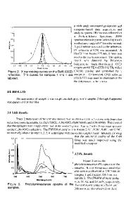
to monitor the growth temperature. A closed loop vacuum pumping system enables the reactor to be operated over a pressure range of 10 to 760 torr with good stability. A high vacuum loadlock is interfaced to the reactor to isolate it from the ambient environment during wafer loading and unloading operations. Figures 1(b) and (c) show the original Figure 1. (a) schematic of the MOCVD reaction chamber. (b) and modified susceptor, respectively. The original, original susceptor shape. (c) modified susceptor shape. manufacturer-supplied susceptor has a diameter of 37.5 mm, including a circular central part (which has a diameter of 25.5 mm) and an outer edge of 6 mm width. The central part of the modified susceptor was unchanged from the original, but the outer edge was cut and tapered. The diameter at the base of the modified susceptor was 31.5 mm. The source gases were ammonia (NH3), trimethylgallium (TMGa), and trimethylaluminum (TMA). Hydrogen was used as a carrier gas. Silicon (111) was used as the substrate, and it was cleaned in acetone, 2%HF, and UHP deionized water, then dried with N2. Prior to growth, it was heate
Data Loading...