Electrical Characterization of GaN Metal Oxide Semiconductor Diode using Sc 2 O 3 as the Gate Oxide
- PDF / 67,195 Bytes
- 6 Pages / 612 x 792 pts (letter) Page_size
- 92 Downloads / 350 Views
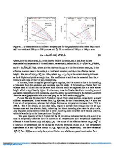
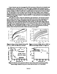
Electrical Characterization of GaN Metal Oxide Semiconductor Diode using Sc2O3 as the Gate Oxide R. Mehandru1, B.P. Gila2, J. Kim1, J.W. Johnson1, K.P. Lee2, B. Luo1, A.H. Onstine2, C. R. Abernathy2, S.J. Pearton2, and F.Ren1 1. Department of Chemical Engineering, University of Florida, Gainesville, FL 32611, USA. 2. Department of Materials Science and Engineering, University of Florida, Gainesville, FL 32611, USA. Abstract GaN metal oxide semiconductor diodes were demonstrated utilizing Sc2O3 as the gate oxide. Sc2O3 was grown at 100 °C on MOCVD grown n-GaN layers in a molecular beam epitaxy (MBE) system, using a scandium elemental source and an Electron Cyclotron Resonance (ECR) oxygen plasma. Ar/Cl2 based discharges was used to remove Sc2O3, in order to expose the underlying n-GaN for ohmic metal deposition in an Inductively Coupled Plasma system. Electron beam deposited Ti/Al/Pt/Au and Pt/Au were utilized as ohmic and gate metallizations, respectively. An interface trap density of 5 × 10¹¹ eV-1cm-2 was obtained with the Terman method. Conductance-voltage measurements were also used to estimate the interface trap density and a slightly higher number was obtained as compared to the Terman method. Results of capacitance measurements at elevated temperature (up to 300°C) indicated the presence of deep states near the interface. Introduction GaN is regarded as having tremendous potential for applications in high temperature, high power and high speed electronic devices[1,2]. Though it has a large band gap, the device performance degrades at higher temperature due to high gate leakage resulting from limited Schottky barrier height. Many insulators, such as Ga2O3 (Gd2O3), AlN, SiO2 or Si3N4, have been proposed for use in GaN-based metal oxide semiconductor field effect transistors (MOSFETs) structures[2-13]. Some of them are known to have very high breakdown field, but they all have a large lattice mismatch, resulting in a relatively high interface state density for crystalline oxides. For example, Gd2O3, which has a bandgap of 5.3eV, has a large lattice mismatch of ~20% to GaN. Sc2O3 has a similar bixbyite structure but it also has a larger bandgap of 6.3 eV and a smaller lattice mismatch ~9.2%. In this work, scandium Oxide (Sc2O3) was deposited as gate insulator on GaN. Electron microscopy showed the resulting interface to be smooth. MOS diodes were fabricated and characterized with current-voltage (IV), capacitance–voltage (CV) and conductance-voltage (GV) measurements. CV measurements under ultraviolet light and at higher temperature were also performed. Experimental Scandium oxide was deposited epitaxially on (0001) GaN in a molecular beam epitaxy system (MBE) using elemental Sc and an electron cyclotron resonance (ECR) oxygen plasma. All oxide growths were performed in a modified RIBER 2300 MBE equipped with a reflection I11.47.1
high-energy electron diffraction (RHEED) system. Oxygen was supplied from a Wavemat MPDR 610 ECR plasma source (2.54 GHz) with 200-Watts forward power at 1x10⁻⁴ Torr. oxygen pressure.
Data Loading...