Electrical Transport in Carbon Nanotube Y-junctions- a Paradigm for Novel Functionality at the Nanoscale
- PDF / 525,858 Bytes
- 6 Pages / 612 x 792 pts (letter) Page_size
- 8 Downloads / 319 Views
0922-U11-08
Electrical Transport in Carbon Nanotube Y-junctions- a Paradigm for Novel Functionality at the Nanoscale Jeongwon Park1, Chiara Daraio1, Apparao Rao2, and Prabhakar Bandaru1 1 Materials Science program, UC, San Diego, La Jolla, CA, 92093-0411 2 Clemson University, Clemson, SC, 29634-0978 ABSTRACT Carbon Nanotube (CNT) morphologies with a self-contained gate, such as Y-junctions, offer a new way of exploiting the features unique to the nanoscale, such as quantum ballistic transport. The advantages of low power and high frequency operation can then be applied to the fabrication of novel devices. Several other novel functionalities in Y- CNTs, including rectification, switching, high-frequency performance, and logic gates have been experimentally verified1. Y-CNT geometry dependent current blocking behavior, as a function of annealing temperature has also been observed. In view of the above observations, this paper proposes that Y-CNTs can be used for prototypical nanoelectronic components.
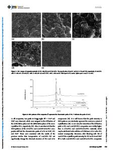
INTRODUCTION Carbon Nanotube (CNT) based electronics offer significant potential, as a nanoscale alternative to silicon based devices, for novel molecular electronics technologies2. The advantages of much lower resistance, higher thermal conductivity, and the possibility of new devices using novel physical principles can be judiciously used for the development of new paradigms in nanotechnology. So far, the elucidation of fundamental properties of nanotubes and nanowires and their applicability for electrical devices has mainly focused on adopting the MOSFET3, 4 (Metal-Oxide Semiconductor Field Effect Transistor) paradigm, where a nanotube serves as the channel between lithographically fabricated electrodes (viz., Source and Drain), and an electrically insulated gate modulates the channel conductance. In other demonstrations, cumbersome Atomic Force Microscope (AFM) manipulations5 of nanotube properties have been utilized. To take advantage of the inherent/intrinsic properties of nanotubes, a fully integrated nanotube electronics, where both devices and interconnects are based on CNTs, is desired. In the present work, we focus on the electrical measurements on a particular multi-walled CNT
(MWNT) morphology- the Y-junction- grown by modified chemical vapor deposition (CVD) processes6. We have observed1 unique switching behavior and the promise of using this element as a new type of logic device. In this paper, we report on the high frequency behavior and novel rectification properties induced through high temperature annealing in Y-CNT structures. EXPERIMENTAL DETAILS The Y-junction nanotubes were grown on bare quartz or SiO2/Si substrates through thermal Chemical Vapor Deposition (CVD). A mixture of ferrocene (C10H10Fe), xylene (C10H10) and a Ti containing precursor gas-C10H10N4Ti was decomposed at 750 oC in the presence of flowing argon (~ 600 sccm) and hydrogen (75 sccm) carrier gases. The CVD reactor consists of two stages: (1) a low temperature (~ 200 oC) preheating chamber for the liquid mixture vaporization fol
Data Loading...