Imaging Schottky Barriers at Carbon Nanotube Contacts
- PDF / 694,306 Bytes
- 6 Pages / 612 x 792 pts (letter) Page_size
- 25 Downloads / 364 Views
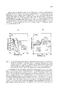
Imaging Schottky Barriers at Carbon Nanotube Contacts Marcus Freitag and A. T. Johnson Department of Physics and Astronomy, University of Pennsylvania, Philadelphia, Pennsylvania 19104 ABSTRACT We use scanning gate microscopy to precisely locate the gating response in single-wall nanotube devices. Junctions of metallic and semiconducting nanotubes show a dramatic increase in transport current when they are electrostatically doped with holes at the junction. We ascribe this behavior to the turn-on of a reverse biased Schottky barrier. A similar effect is seen in fieldeffect transistors made from an individual semiconducting single-wall carbon nanotube. In this case, there are two Schottky barriers at the metal contacts, one of which is forward, and one of which is reverse biased. The gating action is only observed at the reverse biased Schottky barrier at the positive electrode. By positioning the gate near one of the contacts, we convert the nanotube field-effect transistor into a rectifying nanotube diode. These experiments both clarify the gating mechanism for nanotube devices and indicate a strategy for diode fabrication based on controlled placement of acceptor impurities at a nanotube field-effect transistor.
INTRODUCTION Single-wall carbon nanotubes (SWNTs) are promising components for nano-electronic circuits. Metallic (M-) SWNTs are ballistic quantum wires [1] and could serve as onedimensional interconnects between molecular devices. Semiconducting (SC-) SWNTs have been shown to function as molecular field-effect transistors (FETs) [2]. They can be converted into diodes by localized impurities [3] or alkali dopants [4]. Junctions of metallic and semiconducting nanotubes have a rectifying behavior, presumably due to a Schottky barrier at the junction [5]. Semiconducting SWNTs exposed to atmosphere typically show hole transport [6]. N-type doping into the metallic regime occurs upon doping with potassium [7-9]. Moreover, charge transfer between metal contacts and the nanotube shifts its chemical potential and leads to band bending in the nanotube. Band bending is predicted to occur over nanometer length scales for heavily doped nanotubes or micrometers for nearly depleted nanotubes [10]. Contradictory models have been proposed to explain FET action in semiconducting nanotubes. Tans et al. suggested that the nanotube valence band was pinned at the Fermi level of the leads and "sagged" away from the contacts to produce a barrier to hole transport in the middle of the device [2]. A fundamentally different model was suggested for the junction between crossed SWNTs, one metallic and one semiconducting [5]. A Schottky barrier at the nanotube–nanotube contact was proposed, with the rest of the semiconducting nanotube doped to a conductive state. Here we resolve this issue by directly probing the local field effect in a M-SC nanotube junction and in a nanotube field-effect transistor [11] using a scanning gate microscope (SGM). The method has previously been used to reveal semiconducting areas in nanotube bundles [12
Data Loading...