Electron, Ion and Photon Beam Processing
- PDF / 2,067,543 Bytes
- 9 Pages / 420.48 x 639 pts Page_size
- 119 Downloads / 388 Views
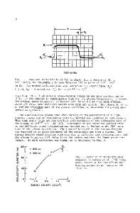
ELECTRON, ION AND PHOTON BEAM PROCESSING KENJI GAMO Faculty of Engineering Science and Research Center for Extreme materials, Osaka University, Toyonaka, Osaka 560, Japan ABSTRACT Beam processing techniques are increasingly important because of their unique capability as nano-device fabrication techniques. These are low temperature processing, high spacial resolution, high material and spacial selectivity and anisotropy, etc. For device fabrication, reduction of processinduced damage is crucial. In the present paper, basic characteristics of electron, ion and photon beam processing for etching and deposition are compared with putting emphasize on the effect of damage and promising techniques to minimize damage. INTRODUCTION With continuous scale down of microelectronic devices, beam processing techniques which uses electron, ion and photon beams become increasingly important. This is first because very fine pattern fabrication is required for future devices. Various beam processing can fabricate nanostructures. Minimum pattern size fabricated so far is -4nm for electron beams[I], -12nm for focused ion beams[2] and -17nm for X-ray[31. These patterns are fabricated by lithography processing, but may be also achieved by other techniques. Second, low temperature is required for any processing to minimize thermal stress and interface reaction which degrade device performance. Beam processing is promising to lower various processing temperatures, for example, film deposition temperature and epitaxy temperature. Third very high processing accuracy and reliability can be expected for beam processing. We can expect an atomic-layer precision for deposition and etching, and fourth, areal and material selectivity can be obtained using beam processing. All processes should be performed without introducing damage. This should be major problem, especially for ion beam processing. ETCHING AND DEPOSITION Maskless or selective area etching and deposition are one of the most important advantages of beam processing. This is realized by beam assisted etching and beam induced chemical vapor deposition or beam assisted deposition techniques, where beams are irradiated to induce locally various reaction steps affecting etching and deposition process. Electron beam assisted etching may be promising to fabricate fine pattems with minimal damage creation. Figure 1 shows an example of GaAs pattern formed by electron beam assisted etching[41. In this example, the etching was performed by irradiating electron beams in C02 ambient to form 0.4iim wide, 0.7itm high line pattems. The etched surface is not very smooth. Very careful surface cleaning may be necessary to obtain smooth surface, because the etching proceed by chemical process and a slight contamination at the surface or a thin native oxide layer inhibit the etching. Figure 2 shows an example of a pattern formed in GaAs by ion beam assisted etching[5]. In this example, focused Au ions were irradiated at 60* from the surface normal in Cl2 gas ambient. For the ion beam assisted etching, a v
Data Loading...