Electron Microscope Study of Initial Stage of Growth of ZnSe on GaAs
- PDF / 1,582,511 Bytes
- 6 Pages / 420.48 x 639 pts Page_size
- 60 Downloads / 401 Views
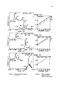
ELECTRON MICROSCOPE STUDY OF INITIAL STAGE OF GROWTH OF ZnSe ON GaAs J. M. Gonsalves(a, N. Otsuka(a, j. Qiu(b M. Kobayashi(b, R. L. Gunshor(b, and L. A. Kolodziejski(c (a) School of Materials Engineering (b) School of Electric Engineering Purdue University, West Lafayette, IN 47907 (c) School of Electric Engineering Massachusetts Institute of Technology Cambridge, MA 02139 Abstract Recent molecular beam epitaxy (MBE) studies have shown that depending on surface conditions of GaAs two different growth modes, layer-by-layer or island, occur at the initial stage of the growth of ZnSe on (100) GaAs. In this study, we have observed various types of GaAs surfaces used for the MBE growth of ZnSe by reflection electron microscopy and ZnSe islands on a GaAs substrate by cross-sectional high resolution electron microscopy. Results of these observations suggest that the occurrence of two growth modes is determined by atomistic structures of GaAs surfaces such as the surface stoichiometry or the density of atomic steps. 1. Introduction In recent years, the growth of II-VI/III-V heterostructures such as ZnSe/GaAs and CdTe/InSb is attracting a great deal of attentions. The combination of II-VI and III-V semiconductors can give rise to wide variations of band gaps as well as close match of lattice parameters and, hence, provides opportunities of developing new novel device structures [1]. One fundamental material problem, however, has to be solved in order to achieve device applications of these heterostructures. It has been pointed out that the chemical bond mismatch between II-VI and II-V semiconductor crystals will result in the formation of inferior interfaces which may have compounds such as Ga 2Se3 or In 2Te3 or a high density interface states [2,3]. In earlier studies of molecular beam epitaxy (MBE) growth of ZnSe [4], Gunshor et al. have observed the layer-by-layer growth mode at the initial stage of the growth of ZnSe on (100) As-stabilized surfaces of GaAs epilayers. They have also observed that ZnSe starts to grow by the island growth mode on bulk GaAs substrate surfaces which are partly Ga-stabilized. In a recent paper on the MBE growth of ZnSe on GaAs [5], Tamargo et al. have reported that the layer-by-layer growth mode occurs on both As-rich epilayer and bulk substrate surfaces, while Ga-rich epilayer and bulk substrate surface give rise to the island growth mode. As known from theories of heterogeneous nucleation [6], the initial growth mode of a thin film is directly affected by the strength of chemical bonds between the overlayer and substrate. Experimental results mentioned above, therefore, suggest the possibility of direct control of the nature of chemical bonds in the ZnSe/GaAs interface by MBE. By this growth technique, the surface stoichiometry of a substrate can be controlled by the use of elemental source fluxes in the ultra-high vacuum system. Along with this capability, low growth temperatures of MBE may enable one to kinetically control the formation of atomic structures of interfaces. Mat. Res. Soc. S
Data Loading...