Electronic and Optoelectronic Applications of Materials Grown at a Low Temperature by MBE
- PDF / 1,628,189 Bytes
- 12 Pages / 420.48 x 639 pts Page_size
- 89 Downloads / 329 Views
ELECTRONIC AND OPTOELECTRONIC APPLICATIONS OF MATERIALS GROWN AT A LOW TEMPERATURE BY MBE U. K. Mishra, ECE Department, UCSB, Santa Barbara, CA. 93106 and R.M. Kolbas, Department of E&CE, NC State University, Raleigh, NC 27695
ABSTRACT: Materials grown at a low temperature by MBE and subsequently annealed at a high temperature have an excess amount of Arsenic and have demonstrated high dielectric breakdown strength and low carrier lifetime. These properties have found applications in analog and switching power applications, in picosecond pulse generation, in device isolation and in the selective intermixing of heterostructures. This paper reviews these applications. 1. INTRODUCTION: Low Temperature GaAs or LT GaAs refers to GaAs grown at a low temperature (typically 200 0 C) by MBE. The material and its initial applications were pioneered by Calawa and Smith at the MIT Lincoln Laboratories. Their work concentrated on material that was grown at 200 0 C and subsequently annealed at 6000C for 10 minutes. This stabilized LT GaAs was found to be highly resistive and optically inactive. These properties have been exploited in a variety of electronic and opto-electronic applications which this paper will attempt to review. 2. ELECTRONIC APPLICATIONS: 2.1 LT Materials as a Buffer. The first application of LT GaAs by Smith etal[1], was as a buffer for a GaAs MESFET. The most dramatic impact as shown in figure 1 was on the virtual elimination of backgating in these MESFETs compared to those fabricated on proton implanted undoped buffers. Sidegating is caused by the injection of carriers from a contact which modify the depletion region at the substrate/channel interface and hence the channel current[2]. This current is suppressed by orders of magnitude by LT GaAs because the large trap density in the material (>101 9 cm-3 ) raises the trap-filled limit voltage, VTFL, before the onset of charge injection. LT buffer technology has also been applied to the AlInAs-GaInAs HEMT system. Brown etal[3], compared the performance of HEMTs with LT AlInAs
Mat. Res. Soc. Symp. Proc. Vol. 241. 01992 Materials Research Society
160
VBG
VDS
J0.15 •m
VOSý 2 5 V SPACING z 50 uýr
Figure 1: Experimental data from Smithetal[1] verifying that LT GaAs as a buffer virtually eliminated backgating in the dark and in the light 08 . compared to conventional buffers. -o,I "-
--
0,
0 I --- ' IMPLANT
04"
SDARK LIGHT
\\
0
,1
TVPE EPITAXIAL LAYER
0 0
-20
-30
BACKGATING VOLTAGE(VI
Ga0.47 In0.53 As
CONTACT
Al0. 4 8 In0 .5 2 As
SCHOTTKY
Ai 0.48ln 0 .5 2 As
DONOR DOSE
AI0. 4 8 1n0.5 2 As
SPACER
Ga0.47 In0.53 As
52
As
2
2
4 x 101 cm"
A.150i
50 A,0 15A 360
CHANNEL
BUFFER
70 A.30oA 315
360
SUPERLATTICE
AlinAs/GalnAs A[0.48 In0
18
5 x 10 cm-3
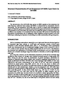
Tgrowth 200°C. 2319,150*C 2397 SAMPLES
InP:Fe SUBSTRATE
Figure 2: The epitaxial layer design and the performance of AlInAs/GaInAs HEMTs with 0.2gtm gate length. The kink effect is effectively suppressed in these devices[3].
2250
161
(grown at 150 0 C and subsequently annealed a
Data Loading...