Engineering the morphology and optical properties of InP-based InAsSb/InGaAs nanostructures via Sb exposure and graded g
- PDF / 52,677,336 Bytes
- 6 Pages / 612 x 792 pts (letter) Page_size
- 91 Downloads / 197 Views
Engineering the morphology and optical properties of InP-based InAsSb/InGaAs nanostructures via Sb exposure and graded growth techniques W. Lei1,2, H.H. Tan1 and C. Jagadish1 1 Department of Electronic Materials Engineering, Research School of Physics and Engineering, The Australian National University, Canberra, Australian Capital Territory 0200, Australia 2 School of Electrical, Electronic and Computer Engineering, The University of Western Australia, Crawley 6009, WA, Australia ABSTRACT Two growth techniques - antimony exposure and graded growth, were proposed to achieve the control over the morphology and optical properties of self-assembled InAsSb/InGaAs/InP nanostructures. By exposing the surface of InGaAs buffer layer to trimethylantimony precursor before the growth of InAsSb nanostructures, the surface/interface energy in the system is reduced, while the strain energy in the system is enhanced. This leads to a change of island shape from dot structure to wire structure. By using a higher initial mole fraction of trimethylantimony precursor during the graded growth of InAsSb, more Sb can be incorporated into the InAsSb islands despite the same Sb mole fraction averaged over the graded growth. This also results in a shape change from dot to wire structure. As a result of their shape change, photoluminescence from the InAsSb nanostructures shows different polarization characteristics. INTRODUCTION Semiconductor InAsSb/InGaAs/InP nanostructures (quantum dots and quantum wires) are promising candidate materials for fabricating mid-infrared (2-3 um) emitters, which have a wide range of applications in military, telecommunications, molecular spectroscopy, biomedical surgery, environmental protection and manufacturing industry, etc.[1-4] Some work has been devoted to growing self-assembled InAsSb quantum dots and extending their emission wavelength.[1-8] However, it is still a big challenge to achieve high quality InAsSb nanostructures with controlled morphology and optical properties due to the large lattice mismatch between InAsSb and InP, surfactant effect of Sb atoms, and low growth temperature requirement for Sb compounds. The widely used approaches to control their morphology and their physical properties are almost all based on changing growth parameters during the growth of these nanostructures, such as growth temperature and growth rate.[6,7,9,10] Little information is known about other controlling techniques.[11] In this work, two novel growth techniques (Sb exposure and graded growth) are proposed to realize the control over the morphology and optical properties of InAsSb nanostructures. The effect of Sb exposure and graded growth on the shape and size of InAsSb nanostructures will be presented and studied. Furthermore, the effect of Sb exposure and graded growth on the photoluminescence polarization characteristic of InAsSb islands will also be discussed.
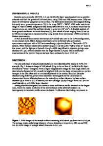
EXPERIMENTAL DETAILS The InAsSb nanostructures were grown on semi-insulating InP (001) substrates in a horizontal-flow metal-organic chemical vapor d