Epitaxial growth of gadolinium oxide on roll-textured nickel using a solution growth technique
- PDF / 2,437,510 Bytes
- 8 Pages / 612 x 792 pts (letter) Page_size
- 81 Downloads / 347 Views
Eliot D. Specht, Amit Goyal, Patrick M. Martin, and Dominic F. Lee Metals and Ceramics Division, Oak Ridge National Laboratory, Oak Ridge, Tennessee 37831
R. Feenstra, D.T. Verebelyi, and D.K. Christen Solid State Division, Oak Ridge National Laboratory, Oak Ridge, Tennessee 37831
Thomas G. Chirayil, Mariappan Paranthaman, Catherine E. Vallet, and David B. Beacha) Chemical and Analytical Sciences Division, Oak Ridge National Laboratory, Oak Ridge, Tennessee 37831 (Received 2 August 1999; accepted 20 December 1999)
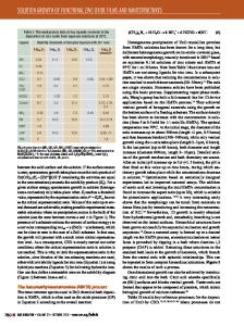
Chemical solution epitaxy was used to deposit an epitaxial film of Gd2O3 on roll-textured nickel. A 2-methoxyethanol solution of gadolinium methoxyethoxide was used for spin-coating and dip-coating. Films were crystallized using a heat treatment at 1160 °C for 1 h in 4% H2/96% Ar. Single-layer films were approximately 600 Å in thickness, and thicker films could be produced using multiple coatings. /2 x-ray diffractograms revealed only (004l) reflections, indicating a high degree of out-of-plane texture. A pole-figure about the Gd2O3 (222) reflection indicated a single in-plane epitaxy. Scanning electron microscopy showed that the films were smooth, continuous, and free of pin holes. Atomic force microscopy revealed an average surface roughness of 53 Å. Electron diffraction indicated that the misalignment of the majority of the grains in the plane was less than 10°. High-current (0.4 MA/cm2) YBa2Cu3O7−␦ films were grown on roll-textured nickel substrates using Gd2O3 as the base layer in a three-layer buffer structure.
I. INTRODUCTION
The next generation of superconducting wire operating at liquid-nitrogen temperature (77 K) is predicted to use a “coated conductor” architecture consisting of a polycrystalline copper oxide superconductor deposited on a mechanically robust metal tape.1 In order to achieve high critical currents in copper oxide superconducting polycrystalline films, it is necessary to have both good outof-plane alignment (c-axis texture, ensuring that the Cu–O planes lie parallel to the substrate) and good inplane alignment (avoiding “weak link” conduction between grains).2 To achieve this alignment in practical coated conductors, two distinctly different approaches to inexpensive substrates are being pursued. One approach involves the deposition of a textured buffer layer on a randomly oriented, oxidation resistant metal tape using multiple ion beams in a technique known as ion beam assisted deposition (IBAD).3 The other approach in-
a)
Address all correspondence to this author. J. Mater. Res., Vol. 15, No. 3, Mar 2000
http://journals.cambridge.org
Downloaded: 16 Mar 2015
volves the deposition of an epitaxial buffer layer on a roll-textured metal tape in a technique known as rollingassisted biaxially textured substrates (RABiTS).4 The first successful RABiTS buffer layer architecture used laser ablation to deposit an epitaxial layer of palladium on roll-textured nickel, followed by a layer of cerium oxide and a layer of yttrium-stabilized zirconia (YSZ).5 Later RABiTS architecture
Data Loading...