Evaluation of electron overflow in nitride-based LEDs influenced by polarization charges at electron blocking layers
- PDF / 775,034 Bytes
- 6 Pages / 612 x 792 pts (letter) Page_size
- 15 Downloads / 300 Views
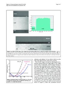
Evaluation of electron overflow in nitride-based LEDs influenced by polarization charges at electron blocking layers K. Hayashi1.T. Yasuda1. S. Katsuno1. T.Takeuchi1. S. Kamiyama1. M. Iwaya1 and I. Akasaki1,2. 1 Faculty of Science and Technology, Meijo University, Nagoya, 468-8502, Japan 2 Akasaki Research Center, Nagoya University, Nagoya, 464-8062, Japan ABSTRACT We have investigated an influence of positive polarization charges generated at an interface between GaN barrier/p-AlGaN EB (Electron Blocking) layer in a blue-LED. Simulation results suggested that such polarization charges caused an electron overflow from QWs. The simulation results also indicated that sufficient acceptor doping at the interface could neutralize the positive polarization charges and suppress the electron overflow. We then demonstrated the electron overflow caused by the positive polarization charges and its suppression with sufficient Mg doping at the interface by monitoring emissions from an additional second QW inserted between the p-EB layer and the p-GaN layer. Finally we conclude that the contribution of the electron overflow is not significant for the efficiency droop in blue-LEDs. INTRODUCTION In GaInN-based blue LEDs, the quantum efficiency is decreased with an increase of a current injection. This phenomenon, the so-called "efficiency droop", is a severe problem for high-power solid-state lighting applications since the LEDs operate under high injection currents [1,2]. A couple of mechanisms, such as carrier overflow from active region [3,4], Auger recombination [5], and carrier spilling over from In rich region have been suggested. However, it is difficult to directly observe such mechanisms with conventional device structures. Very recently hot electrons generated by the Auger recombination were directly observed by electron emission spectroscopy [6]. Also, a few reports on the direct measurement of electron overflow have been published [7-9]. In the measurement, an additional second active region to capture the overflowing electrons were inserted in p-layers. The overflowing electrons captured at the second active region recombine with holes, resulting in light emissions. By monitoring the light emissions, the electron overflow can be directly measured. In the meantime, positive polarization charges at an interface between a GaN barrier and a p-AlGaN EB layer were concerned as an origin of electron overflow [10]. At the interface of Al0.2Ga0.8N/GaN, 1×1013 cm-2 positive seat charge density is generated. Such positive polarization charges could lower the conduction band energy level, and promote the electron overflow. At the same time such positive polarization charges could be neutralized with the negative charges which are ionized acceptors for the case in the p-layer. For instance, the total amount of the negative charges from the ionized acceptors in a 10 nm Mg-doped GaN with 1×1019 cm-3 is equal to that of the positive charges from the polarization effect at the interface of the Al0.2Ga0.8N/GaN, 1×1013 cm-2. Thus suffici
Data Loading...


