Chemical characterization of extra layers at the interfaces in MOCVD InGaP/GaAs junctions by electron beam methods
- PDF / 1,270,969 Bytes
- 7 Pages / 595.276 x 793.701 pts Page_size
- 76 Downloads / 300 Views
NANO EXPRESS
Open Access
Chemical characterization of extra layers at the interfaces in MOCVD InGaP/GaAs junctions by electron beam methods Cesare Frigeri1*, Alexey Aleksandrovich Shakhmin2, Dmitry Anatolievich Vinokurov2, Maria Vladimirovna Zamoryanskaya2
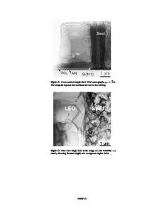
Abstract Electron beam methods, such as cathodoluminescence (CL) that is based on an electron-probe microanalyser, and (200) dark field and high angle annular dark field (HAADF) in a scanning transmission electron microscope, are used to study the deterioration of interfaces in InGaP/GaAs system with the GaAs QW on top of InGaP. A CL emission peak different from that of the QW was detected. By using HAADF, it is found that the GaAs QW does not exist any longer, being replaced by extra interlayer(s) that are different from GaAs and InGaP because of atomic rearrangements at the interface. The nature and composition of the interlayer(s) are determined by HAADF. Such changes of the nominal GaAs QW can account for the emission observed by CL. Introduction Several devices, such as HBTs, HEMTs, solar cells and LEDs, are currently based on InGaP/GaAs heterojunction because of its superior properties with respect to AlGaAs [1-4]. The InGaP/GaAs system, especially if it is grown by metal organic vapour phase deposition (MOCVD), has, however, the drawback that the interfaces between InGaP and GaAs are deteriorated, as shown by photoluminescence, X-ray diffraction and transmission electron microscopy (TEM), because there is no common group V element across the interface [5]. This mostly affects the inverted GaAs-on-InGaP interface where an unwanted extra interlayer forms, which recombines the minority carriers more efficiently than the GaAs quantum well [5-10]. The normal InGaP-onGaAs interface is always good, but this is not sufficient to guarantee reliable device performance. The deterioration of the inverted GaAs-on-InGaP interface has been seen to occur in practically every MOCVD InGaP/GaAs heterostructure containing such an interface, to a more or less great extent depending on the growth conditions [5-10]. It could sometimes be avoided by the use of growth interruption between the layers [6], the growth * Correspondence: [email protected] 1 CNR-IMEM Institute, Parco Area delle Scienze 37/A, 43010 Parma, Italy Full list of author information is available at the end of the article
on top of InGaP of a thin (1 nm) intentional interfacial layer of GaP [5,7,9] or GaAlAs [8], or the application of a preflow of trimethylgallium on the InGaP surface before switching on the AsH3 flow [11]. A recent contribution to this field was based on cathodoluminescence (CL) measurements [12,13]. The difference between the two interfaces was confirmed by comparing two InGaP/GaAs systems containing a GaAs QW and either one of the two interfaces [12,13]. One sample had the layer sequence GaAs substrate/GaAs buffer/AlGaAs/GaAs/InGaP with the normal interface. It showed the expected GaAs QW emission (1.56 eV at 77 K). The other sample had the sequence GaAs substrate/GaAs buffer/InGaP/GaAs
Data Loading...