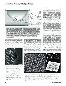
Exploring Surfaces of Materials with Atomic Force Microscopy
Several aspects of Atomic Force Microscopy (AFM) are considered in this chapter. Theoretical backgrounds of AFM, which are based on the asymptotic solution of tip–sample interactions, lead to the classification of modes and computer simulations of images
- PDF / 2,581,953 Bytes
- 51 Pages / 439.37 x 666.142 pts Page_size
- 46 Downloads / 389 Views
Exploring Surfaces of Materials with Atomic Force Microscopy S. Magonov, J. Alexander, and S. Belikov
Abstract Several aspects of Atomic Force Microscopy (AFM) are considered in this chapter. Theoretical backgrounds of AFM, which are based on the asymptotic solution of tip–sample interactions, lead to the classification of modes and computer simulations of images and force curves. Visualization of surface morphology with high resolution is the main AFM application. The practical issues of the highresolution imaging, tracking of corrugated surfaces, and compositional mapping of multicomponent polymers are illustrated in several examples. The components of heterogeneous systems are recognized by their specific shape or by their different mechanical and electric properties revealed in the AFM-based methods. The challenges of the quantitative nanomechanical studies of soft materials are discussed. The multifrequency examination of local electric/dielectric properties is presented by the single-pass studies of surface potential and dielectric response on various samples.
7.1
Introduction
Microscopic studies of surfaces were revolutionized over 30 years ago with the invention of the scanning tunneling microscope (STM) [1]. In this device the detection of tunneling current between a sharp metallic tip and a (semi)conducting surface is applied for visualization of surface structures with atomic-scale resolution. Although the novel microscope has the same basic components of the earlier introduced topographiner [2], the innovative STM applications have advanced microscopic studies tremendously. At the beginning, the high-resolution visualization of surface structures with STM was restricted due to the need for sample conductivity. This limitation was removed when Atomic Force Microscopy (AFM) was introduced for
S. Magonov (*) • J. Alexander • S. Belikov NT-MDT Development Inc., 430 W. Warner Rd., Tempe, AZ 85284, USA e-mail: [email protected] A. Korkin and D.J. Lockwood (eds.), Nanoscale Applications for Information 203 and Energy Systems, Nanostructure Science and Technology, DOI 10.1007/978-1-4614-5016-0_7, # Springer Science+Business Media New York 2013
204
S. Magonov et al.
studies of surfaces with the use of more universal tip–sample forces [3]. In this technique, a micro-fabricated probe consisting of a cantilever with a sharp pyramidal tip at its free end serves as a sensor of forces acting between the tip apex (3–20 nm in diameter) and a sample surface. The tip–sample interactions are measured by the deflection of the cantilever that is monitored by an optical lever scheme [4]. At present, there are a number of different AFM scanning modes, in which the probe stays either in permanent contact with a sample or interacts intermittently, being driven into oscillatory motion. The changes of the cantilever deflection and oscillatory parameters (amplitude, frequency, phase) can be employed for monitoring tip–sample force interactions. For surface profiling, the probe or the sample is moved laterally, and the feedb
Data Loading...