Fabrication and Characterization of Cold Electron Emitter Based on Nanocrystalline Silicon Dots
- PDF / 328,690 Bytes
- 5 Pages / 612 x 792 pts (letter) Page_size
- 88 Downloads / 234 Views
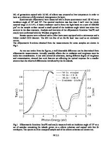
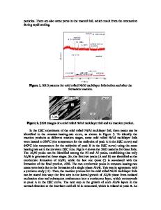
FABRICATION AND CHARACTERIZATION OF COLD ELECTRON EMITTER BASED ON NANOCRYSTALLINE SILICON DOTS K. Nishiguchi1, X. Zhao2, and S. Oda1 1 Research Center for Quantum Effect Electronics, Tokyo Institute of Technology, 2-12-1 O-okayama, Meguro-ku, Tokyo 152-8552, Japan 2 Department of Physics, Science University of Tokyo, 1-3 Kagurazaka, Shinjuku-ku, Tokyo 162-8601, Japan ABSTRACT A cold electron emitter has been made from nanocrystalline silicon (nc-Si) dots. Nc-Si dots are formed in the gas phase by very-high-frequency (VHF) plasma enhanced chemical vapor deposition (CVD). Electrons, accelerated by electric field, are ballistically transported through nc-Si and SiO2, then extracted into vacuum. Electron emission efficiency is optimized through varying nc-Si film thickness, surface roughness, and by short thermal oxidation. INTRODUCTION Recently, cold electron emitting devices have been studied intensively for their use in flat panel type displays. The electron emitters formed by silicon or metal cones based on a field emission effect have been demonstrated but have unacceptably low efficiency and are difficult to focus to a small point.1,2 An electron emitter using carbon nanotubes shows a very high emission efficiency, however, lifetime is ultimately reduced by oxidation even if it is operated in vacuum.3,4 Moreover, field emission devices require high vacuum, which leads to a difficult fabrication. A planer type electron emitter with narrow beam dispersion formed by porous Si (PS) has also been proposed to overcome the problems mentioned above.5 The authors suggest that the dominant mechanism is hot electrons ballistically transported through the PS layer. An external quantum efficiency, defined by the ratio of the emission current to the total currents, of about 1% was achieved. In this case, a wet etching process was used. This makes both investigating mechanism and improving the device performance difficult. The direct deposition of uniform nc-Si material is expected to be a promising candidate of fabricating high efficiency electron emitters. The nc-Si thin films have been fabricated by using VHF plasma CVD with well-controlled crystal sizes.6 In this paper, we present a planar type nc-Si electron emitter formed by VHF plasma CVD. In this system, we can deposit Si nano-scale dots with well controlled sizes and smooth surface morphology to arbitrary substrates in dry process. A high emission efficiency comparable to PS is obtained. FABRICATION An n+-Si (0.01Ωcm) wafer was used as the substrate and the electron source. The nc-Si dots with diameters of 10±5 nm were deposited onto the substrate at room temperature by plasma CVD. Figure 1 shows the fabrication system of nc-Si dots. The CVD system includes a plasma cell, which is separated from UHV chamber by a stainless steel plate with 6mm-diameter orifice. Ar and SiH4 gases, whose flow rates were 10 sccm and 1 sccm, respectively, are excited by a 144MHz plasma with a power of 3W. The nc-Si dots were formed in the gas phase by coalescence of SiH4-derived radicals an
Data Loading...