Fabrication and Characterization of Thin-Film Metal-Insulator-Metal Diode for use in Rectenna as Infrared Detector
- PDF / 2,811,656 Bytes
- 8 Pages / 612 x 792 pts (letter) Page_size
- 62 Downloads / 241 Views
0935-K03-18
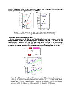
Fabrication and Characterization of Thin-Film Metal-Insulator-Metal Diode for use in Rectenna as Infrared Detector Subramanian Krishnan, Shekhar Bhansali, Kenneth Buckle, and Elias Stefanakos Electrical Engineering, University of South Florida, 4202 E.Fowler Ave., ENB118, Tampa, FL, 33620 Abstract Planar, asymmetric, thin-film Ni-NiO-Cr metal-insulator-metal (MIM) diodes with 1µm2 contact area were fabricated using E-beam lithography with cut-off frequency in the millimeter-wave regime (0.1THz). The electrical behavior of the detector was observed and verified with a theoretical model. By measuring the I-V characteristics of the diode, a higher degree of nonlinearity was demonstrated. For devices with such non-linear electrodes, excellent agreement is obtained between measured and calculated results with current ranging from 0.8mA to 0.2mA at 0.2V. Introduction High-frequency switching diodes have been explored and investigated for their application as IR detectors. When compared to bolometers, antenna-coupled MIM diodes offer significant advantages such as high sensitivity and faster rectification response [1]. These high-frequency diodes are realized by utilizing the Metal-Insulator tunnel junctions, operating on the basis of quantum mechanical phenomena. When a sufficiently thin barrier is sandwiched between two electrodes, electrons tunnel through the barrier layer causing a current flow [2]. This tunnelling probability increases with a decrease in the dielectric barrier height and the insulator thickness [3]. MIM diodes with similar metals such as Ni-NiO-Ni and Al-Al2O3-Al have been fabricated and tested [4, 5] -coupled with an antenna for Infrared detection. In this paper, we report the fabrication and characterization of MIM diode using dissimilar metals (Ni-NiO-Cr) with contact areas of 1µm2 to achieve non-linear dc characteristics with operating frequency ~ 0.1THz. Besides, the insulator layer was characterized to yield a uniform thin-film (~5nm). In addition, scanning electron microscopy (SEM) and atomic force microscopy (AFM) were employed to analyze the morphology of the diode and the roughness of the dielectric, respectively. Experimental Design Techniques The most important factor to be considered in the design of the MIM tunnel diode is the size of the contact area between the metal layers and the insulator layers. The capacitance and hence the active area of the diode can be determined by replacing the desired value of cut-off frequency in the equation below: 1 (1) C d = εoεrA fc =
2 ∏ R aC d
d
where, Ra and Cd are the input resistance from the antenna and capacitance of the device, respectively; ε0 and εr are the dielectric constant of the NiO and permittivity of free space, respectively; A is the contact area of the MIM diode and d is the thickness of the dielectric. From the above equation, the capacitance and hence the contact area, are calculated to be 34fF and 1.6µm2, for the input resistance ~50Ω. A schematic of the MIM diode is shown in Figure 1.
Figure 1: A Schematic of MIM
Data Loading...