Fabrication of Carbon Nanotube Field-Effect Transistors with Metal and Semiconductor Electrodes
- PDF / 659,996 Bytes
- 7 Pages / 612 x 792 pts (letter) Page_size
- 96 Downloads / 389 Views
1057-II15-20
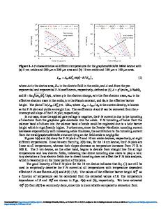
Fabrication of Carbon Nanotube Field-Effect Transistors with Metal and Semiconductor Electrodes Himani Sharma, and Zhigang Xiao Department of Electrical Engineering, Alabama A & M University, 4900 Meridian Street, Normal, AL, 35762 ABSTRACT Carbon nanotube field-effect transistors (CNTFETs) were fabricated with metal material (gold) and semiconductor material (bismuth telluride) as the source and drain materials. Highly-purified HiPCO-grown single-walled carbon nanotubes (CNTs) from Carbon Nanotechnologies, Inc. (CNI) were used for the fabrication of CNTFETs. The singlewalled carbon nanotubes were ultrasonically dispersed in toluene and dimethylformamide (DMF) with trifluoroacetic acid (TFA), as co-solvent. Dielectrophoresis (DEP) method was used to deposit, align, and assemble carbon nanotubes (CNTs) to bridge the gap between the source and drain of CNTFETs to form the channel. The structure of CNTFET is similar to a conventional field-effect transistor with substrate acting as a back-side gate. Electron-beam evaporation was used to deposit gold and bismuth telluride thin films. Microfabrication techniques such as photolithography, e-beam lithography, and lift-off process were used to define and fabricate the source, drain, and gate of CNTFETs. The gap between the source and drain varied from 800 nm to 3 µm. The drain-source current (IDS) of the fabricated CNTFETs versus the drain-source voltage (VDS) and the gate voltage (VG) was characterized. It was found that in the case of gold (Au) electrodes, the I-V curves of CNTFETs clearly show behavior of the CNT (metallic or semiconducting) aligned across the source and drain of CNTFETs, while in the case of bismuth telluride (Bi2Te3) electrodes, the I-V curves are less dependent on the type of CNTs (metallic or semiconducting). The developed carbon nanotube field-effect transistors (CNTFETs) can be a good candidate for the application of nanoelectronics and integrated circuits with a high mobility and fast switching. INTRODUCTION Single walled carbon nanotubes (SWNTs) have been the subject of extensive research for their unique chemical, mechanical, electronic properties and thus their potential applications in molecular electronic devices [1,2], such as field emitted displays, fuel cells, transistors and chemical or biosensors [3-7]. Metallic carbon nanotubes, which appear to be ballistic conductors on a length scale up to microns with critical current densities of 109 A/cm2 are ideal nanoscale wires [8], where as semiconducting nanotubes enable us to build nanoscale field-effect transistors [9]. A major problem in the realization of electronic circuits is the difficulty to position and contact carbon nanotubes in a controlled way. Several methods have been reported so far, including (a) spraying of nanotubes [9, 10] onto Si substrate prior to or after lithographic structuring of metallic contacts; (b) catalytic growth of nanotubes [11] on desired substrate using predeposited catalyst islands; (c) or selective deposition of carbon nanotubes on chemically
Data Loading...