Formation of Buried Two-Dimensional Electron Gas in Gaas by Si Ion Doping Using Mbe-Fib Combined System
- PDF / 797,576 Bytes
- 5 Pages / 414.72 x 648 pts Page_size
- 19 Downloads / 279 Views
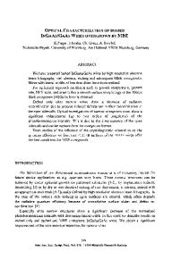
ABSTRACT 0.1 and 30 keV Si 2+ focused ion beams (FIB) were implanted in two types of GaAs, one of which is semi-insulating (s.i.) GaAs, while the other is grown by molecular beam epitaxy (MBE). Successive regrowth over the implanted surface was performed using MBEFIB combined system, and the resistance was measured. It was found that for 100 eV Sil+ FIB implantation, the sample was nonconductive without a post annealing at 800'C. After the post annealing, however, the sample became conductive and the resistance was the same order in magnitude as the sample fabricated using 30 keV S0i+ FIB irradiation. This suggests "apotential of selective formation of Si 6-like doped layers in GaAs and GaAs/AlGaAs using "alow-energy FIB. INTRODUCTION Formation of buried nanostructures such as a laterally-confined two-dimensional electron gas (2DEG) in semiconductor materials is a key for future development of microelectronics. Buried structures, such as a vertically-coupled electron wave guide1 , can be fabricated by molecular beam epitaxy (MBE) growth before and after a maskless doping by focused ion beam (FIB) implantation using in situ MBE-FIB fabrication systems 2- 7 . In these systems, FIB and MBE chambers are usually connected through an ultra high vacuum (UHV) sample transfer tunnel. Using such systems, samples can be transfered between the two chambers without exposure to air for the maskless implantation, and contamination can be minimized. However, there still remain several problems in this process to be solved. These are interface properties such as trapping behavior at the interface during growth interruption, ion irradiation induced damage, determination of optimum implantation parameters in GaAs, and so on. In the present study, in order to reveal the possibility of selective formation of 2DEG layers in GaAs and GaAs/AIGaAs systems, 0.1 and 30 keV Si 2+ FIB was implanted in semiinsulating(s.i.) and MBE-grown-GaAs samples, and GaAs layers were successively regrown after the implantation. The implanted and regrown layers were characterized by measuring resistances before and after post annealing at 800'C. EXPERIMENT In this experiment, s.i.-GaAs (100) wafers were cut into about 5 mm square chips. After the chips were cleaned using organic solvents and ultra pure water, they were mounted on two Mo blocks using indium solder. Maskless ion implantation and MBE growth were performed using combined systems as shown in Fig.1. The chips were heated to 630'C for 10 min in an arsenic atmosphere to remove native oxides of the chips in the MBE chamber. One group (Group I) was directly transfered to the FIB chamber through the UHV sample transfer tunnel at a pressure of 9x10⁻⁹ Torr after the chips were cooled down. In another group (Group II), undoped, ljsm thick GaAs buffer layer was overgrown at 580'C before they were transfered to the FIB chamber. In the FIB chamber, Sil+ ions were implanted in an area of 600 jimx 3 mm on the GaAs samples at room temperature, as shown in Fig.2. The pressure of the FIB chamber was 701 Mat. Res.
Data Loading...