Formation of TiSi 2 on nitrogen ion implanted (001)Si
- PDF / 447,156 Bytes
- 9 Pages / 612 x 792 pts (letter) Page_size
- 95 Downloads / 391 Views
MATERIALS RESEARCH
Welcome
Comments
Help
Formation of TiSi2 on nitrogen ion implanted (001)Si S. L. Cheng and L. J. Chen Department of Materials Science and Engineering, National Tsing Hua University, Hsinchu, Taiwan, Republic of China
B. Y. Tsui Electronics Research and Service Organization, Industrial Technology and Research Institute, Hsinchu, Taiwan, Republic of China (Received 16 October 1997; accepted 12 March 1998)
Formation of TiSi2 on nitrogen ion implanted (001)Si has been investigated. Nitrogen ion implantation was found to suppress the B and As diffusion in silicon. For Ti on 30 keV BF2 1 –20 keV N2 1 and 30 keV As1 –20 keV N2 1 implanted samples, a continuous low-resistivity TiSi2 layer was found to form in all samples annealed at 700–900 ±C. For Ti on 1 3 1015ycm2 N2 1 - and As1 implanted samples, end-of-range defects were completely eliminated in all samples annealed at 700–900 ±C. The results indicated that with appropriate control, N1 -implantation can be successfully implemented in forming low-resistivity TiSi2 contacts on shallow junctions in deep submicron devices.
I. INTRODUCTION
II. EXPERIMENTAL PROCEDURES
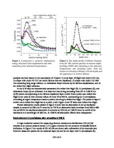
Shallow junction formation has long been one of the major challenges in the fabrication of ultralarge scale integrated circuit (ULSI) devices.1 Recently, nitrogen implantation was used in deep submicron devices to suppress the B and As diffusion as well as hot-carrier degradation.2,3 Preamorphization of silicon was reported to be effective in suppressing channeling in Si.4,5 However, it is not effective for suppressing transient enhanced diffusion (TED). N1 implantation was introduced in an attempt to suppress both channeling and TED.6 For self-aligned silicidation devices, silicides are formed on source, drain, and gate regions simultaneously to ease the lithography requirements and to lower the contact resistance. Low-resistivity TiSi2 is perhaps the most attractive candidate for the self-aligned technology of ULSI circuits because it possesses the lowest resistivity among all silicides, low contact resistance, and good thermal properties as well as compatibility with the self-aligned silicidation process.7,8 As the device dimensions scale down to a deep submicron region, it is essential to understand the interactions of metal contacts with highly doped shallow junctions.9 In addition, the morphological stability of C54–TiSi2 during high temperature annealing is crucial to the development of ULSI technology. In this paper, results from an investigation on the TiSi2 contacts on shallow junctions formed with nitrogen implantation are presented. The n1yp and p 1yn shallow junctions were formed by 30 keV As1 and BF2 1 implants on p- and n-type (001)Si, respectively. The implantation of As1 and BF2 1 on silicon to form shallow junctions is common in ULSI technology.
Single crystal, 3–5 V-cm, (001)Si wafers were used in the present study. Following a standard cleaning procedure, (001)Si wafers were implanted by 30 keV N1 to doses of 5 3 1014 to 1 3 1016ycm2 and 20 keV N2 1 to doses of
Data Loading...