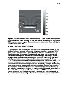
Shallow Junctions Formed by the Thermal Redistribution of Implanted Arsenic into TiSi 2
- PDF / 227,637 Bytes
- 5 Pages / 420.48 x 639 pts Page_size
- 20 Downloads / 313 Views
SHALLOW JUNCTIONS FORMED BY THE THERMAL REDISTRIBUTION OF IMPLANTED ARSENIC INTO TiSi 2 D.X. CAO,
H.B.
HARRISON* AND G.K.
REEVES**
Microelectronics Technology Centre (MTC), Royal Melbourne Technology, 124 LaTrobe Street, Melbourne, Australia 3000. **
Telecom Research Laboratories,
770 Blackburn Road,
Institute
of
Clayton, Australia,3163.
ABSTRACT Following the implantation of arsenic into titanium disilicide films on p type silicon, Rutherford backscattering has shown that rapid thermal vacuum processing (RTVP) causes the arsenic to diffuse toward the silicide/silicon interface, with an accumulation at the interface and with a sharp shallow diffusion into the silicon. The effect of the implant and anneal on the sheet resistance of the silicide and underlying silicon have been investigated' and it 0 is shown that anneal times of thirty seconds at 900 C produce acceptable shallow junctions suitable for device type applications without significant deterioration in silicide electrical or physical properties.
INTRODUCTION One of the non-scaling parameters in integrated circuit fabrication is that of the source, drain extensions and their junction depths. For extremely short extensions it has been shown that antimony is a suitable species if it is ion implanted[l]. However extended source/drain interconnections which are usually silicided still result in comparatively deep junctions because the silicide is usually formed after doping. Another problem which can occur using this technique is a dopant deficiency at the silicide/silicon interface causing poor electrical connection at the interface with a resultant degradation in circuit performance[2]. In an endeavour to circumvent this problem we have first formed the silicide, implanted into it and then used rapid thermal processing to redistribute the dopant species into the silicon. Such a technique was used previously[3] however in that instance co-implants of arsenic and phosphorous were studied. In the following we report our findings along with an explanation of the results.
EXPERIMENTAL Two inch diameter, p type
Data Loading...