GaN P-N Structures Fabricated by Mg ION Implantation
- PDF / 618,472 Bytes
- 6 Pages / 417.6 x 639 pts Page_size
- 102 Downloads / 390 Views
ambient [8, 9]. To date there has been a little work in the area of the device applications of ion implantation in GaN, and generally ion implantation has been used to introduce impurities in GaN for study of their optical properties as well as the damage and passivation processes in GaN [10]. Recently, both n- and p-type GaN, as well as semi-insulating (sheet resistance of >5x 10⁹ W/D-) GaN have been demonstrated by using Si, Mg/P and N ion implantation, respectively, to MOCVD grown GaN with subsequent annealing at 1000-11 00°C for 10 s [11]. In this report, the sheet ptype doping of 9.4x 10"1cm 2 has been achieved at 11 00°C annealing with a Mg activation percentage of -62%, since only 1.53x 1012 cm-2 of the 5x1014 cm 2 implanted acceptors were ionized assuming an energy level of 150 meV for Mg. For Si implantation, the achieved sheet ntype doping of 4.25x 10 3 cm-2 with -93% activation percentage at 1050-1100°C annealing has been reported [ 12]. In addition, high-resistivity layers for increasing the Schottky barrier height were created by implantation Mg, Mg/P and Ca into n-GaN with subsequent activation annealing [13]. The only GaN device fabricated with ion implantation doping up to now is JFET with nchannel and p-gate formed by Si (100 keV, 2x10
14
cm 2 ) and Ca (40 keV, 5x10' 4 cmn2 ) ion
implantation, respectively, and a subsequent 11 50'C 15 s rapid annealing to activate the implanted dopants [14]. Unfortunately, no detailed information on obtained gate junction properties was presented in that work. In the present work an attempt was undertaken to apply ion implantation of Mg into nGaN with subsequent activation annealing to form the p-n structures. Experimental Procedure Epitaxial n-GaN layers were grown by MOCVD on 6H-SiC (0001) substrates with concentration Nd-Na = 3x1018 cm-3. The concentration of the uncompensated donors, Nd-Na, in the GaN layers was (2-3)x1016 cm 3 according to evaluation from Raman measurements like to [15]. Into these n-GaN layers Mg was implanted at energy of 100 keV and at doses in the range from 1013 to 2x1016 cm 2. Samples were annealed for 10-15 s in flowing N 2-gas at a temperatures in the range from 600 to 1200 0 C. The Ohmic contacts to n-SiC and Mg-implanted GaN were produced by vacuum thermal evaporation of Cr/Ni and Pd/Ni, respectively. Ni in the contacts was imployed as a mask during the preparation of 300 ýtm mesas in diameter by reactive ion plasma etching [16]. The thickness of the epilayers, the position of p-n junction inside the structure as well as the absence of the buffer layer at the GaN/SiC boundary were monitored by scanning electron
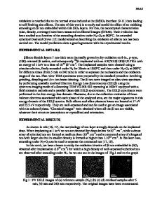
microscopy (SEM). The electron beam induced current (EBIC) and back scattered electron (BSE) techniques were used. Magnesium distribution profiles across the n-GaN layer after ion implantation and annealing were measured using secondary ion mass-spectroscopy (SIMS). The activation process of the Mg acceptors by post-implantation annealing was indicated with a hot point probe method. The current-voltage (I-V) characteristi
Data Loading...