Gate Current Suppressed Lateral FEAs with Integrated TFTs
- PDF / 959,655 Bytes
- 6 Pages / 394.2 x 628.2 pts Page_size
- 90 Downloads / 273 Views
INTRODUCTION In field emitter arrays, the stability of the field emission current is an important issue to practical applications. There have been
considerable efforts to improve the stability and
uniformity of the field emission current employing active devices such as Field-Effect Transistors (FETs) and Thin Film Transistors (TFT)[1-3]. However, most of these devices have four terminals which makes the perimeter circuits complex. In addition, the fabrication process becomes complicated due to the additional process of the integration of active devices, and FEAs and additional area for the active devices are required. In order to overcome these problems, we have reported lateral FEAs with integrated TFTs[4]. The FEAs have stable anode current and three terminals. But the gate current of the FEAs is somewhat large. In this paper, we propose new FEAs which have reduced gate current. The structure of the proposed FEAs(oxide sealed FEAs) is identical to the privious FEAs(metal sealed FEAs) except for the evaporated material. The gate current of the proposed FEAs is negligible compared with the anode current.
143
Mat. Res. Soc. Symp. Proc. Vol. 558 02000 Materials Research Society
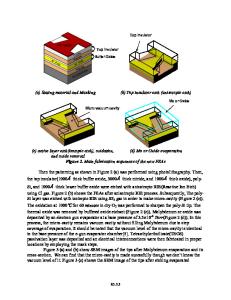
DEVICE STRUCTURE AND FABRICATION Fig. 1 shows the schematic diagram of the metal sealed and oxide sealed FEAs. The main structure of the metal sealed FEAs consists of an n+ poly cathode connected to an undoped polySi tip and the n+ poly anode. The MOS(Metal-Oxide-Semiconductor)-structure is fabricated on the undoped poly-Si tip. The key feature is the undoped tip, the current in which is modulated by the MOS structure. The roles of the gate electrode are vacuum sealing and to modulate the undoped tip, so the device is controllable by the gate electrode[4]. In the metal sealed structure, the gate metal is isolated vertically, but the electrons exit laterally between the tip and the gate metal as shown in Fig. 1 (a). We evaporate oxide instead of metal for vacuum sealing to remove the electron path as shown in Fig. 1 (b).
metal oxide
metal
(b)
(a)
Fig. 1. Schematic diagram of the previous(a) and proposed FEAs(b) The schematic fabrication sequence for the proposed FEA is shown in Fig. 2. The main structure of the oxide sealed FEAs is almost identical to the metal sealed FEAs[4], except for evaporated oxide. We used a Si wafer which was coated with 5000A thick silicon nitride and 500A thick silicon oxide as the starting material. Subsequently, 1000 A thick amorphous Si was deposited on the Si wafer, and 2000A thick silicon oxide was deposited. The 2000A thick silicon oxide was patterned to define undoped region using the first mask, as shown in Fig. 2 (a). The length of the undoped region, that is, the channel length, is 7 /Ma.The 1000A thick amorphous Si was doped with POCI 3 at 9501C, resulting in N+ poly-Si layer having undoped region. The oxide mask was removed, and 3000 A thick silicon oxide was deposited on the active
144
layer(N+ poly-Si layer having undoped region). A part of this silicon oxide corresponding to undoped regio
Data Loading...