Ge Heteroepitaxy on (100) Si Substrates by Ion Assisted Deposition
- PDF / 975,880 Bytes
- 6 Pages / 420.48 x 639 pts Page_size
- 27 Downloads / 349 Views
Ge Heteroepitaxy on (100) Si Substrates by Ion Assisted Deposition
T.G. Holesinger, D.J. Heim, K.M. Lakin, and H.R. Shanks Iowa State University, Microelectronics Research Center Ames, IA.
Abstract Ge films have been grown by ion-assisted deposition on Si(100) substrates. Initial studies were conducted to determine the growth and morphology of Ge using a modified crucible arrangement and ionization chamber. It was observed that a narrow substrate temperature range existed for the deposition of smooth Ge films without ion assistance. Ionization and acceleration appear to induce additional damage to the film without improving crystalline quality.
Introduction The deposition of Ge ?n Si has received considerable attention in recent years. Ge-Si superlattices hold promise for development of novel devices and Ge has also been proposed for use as a buffer layer between Si and GaAs.2,3, GaAs and Si have about a 4% lattice mismatch while the lattice constants of Ge and GaAs are nearly identical. However, Ge films are in general characterized by a high dislocation density. This paper describes an ion-assisted growth technique used in an effort to reduce defects and improve the crystalline quality of Ge films.
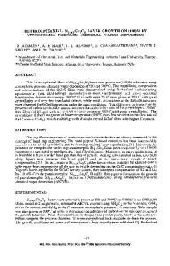
Procedure The Ge films were deposited in a UHV •inized-cluster beam system (ICB) with a base pressure of 1xl0 " torr. A description of this technique can be found elsewhere.5 This system inclgded an insitu ellipsometry system described in an earlier paper. Ge was evaporated from pyrolytic graphite coated carbon crucibles 0 operated at temperatures up to 1850 C. These crucibles had caps with a imm diameter by 1mm thick nozzle. The crucible arrangement along with the ionization and acceleration configuration is shown in Figure 1. The Si wafers used for substrates were first cleaned in l,l,l-trichloroethane (TCE), acetone, and methanol to remove organic contaminants. The substrates were subsequently etched in a dilute HF solution and immediately loaded into the system. The wafers were heated to 800 0 C for 1 hour prior to deposition to desorb the residual oxide. Deposition rates were varied from 0.5 to 5 angstroms per second with film thicknesses ranging from 0.3 to 2 microns. The pressure increased during depositiog, due to outgassing of the source, into the range between ixl0to 5x10 7 torr. The main constituents were nitrogen and hydrogen as monitored by a residual gas analyzer (RGA)
Mat. Res. Soc. Symp. Proc. Vol. 128. t1989 Materials Research Society
286
Ionization and Acceleration
Filament -
Positive Potential (kV)
dia.) -
Heat Shielding Water Cooling
Figure 1)
, Crucible Picket Heater
Crucible, ionization, and acceleration apparatus used for ion-assisted deposition of Ge films.
Characterization The surface morphology was examined using Nomarski and Scanning Electron Microscopes (SEM). Changes in surface morphology and resistivity across the wafer were detected by observing the haze under a high intensity light in conjunction with four-point probe restivity measurements. These observations were then c
Data Loading...