Ge Related Deep Level Luminescence in InGaAs Lattice Matched to InP
- PDF / 212,396 Bytes
- 4 Pages / 420.48 x 639 pts Page_size
- 108 Downloads / 318 Views
Ge RELATED DEEP LEVEL LUMINESCENCE IN InGaAs LATTICE MATCHED TO InP S.S. CHANDVANKAR, A.K.SRIVASTAVA, B.M.ARORA and D.K.SHARMA Tata Institute of Fundamental Research, Homi Bhabha Road, Bombay 400005, India
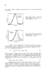
ABSTRACT Photoluminescence and Hall measurements are reported on Ge doped InGaAs layers lattice matched to InP. Ge doping of these samples results in highly compensated material, with the highest Ge content sample giving a p type 7 3 conductivity with carrier concentration of 5x101 cm- . Low temperature PL spectra of these samples show a broad peak from 0.55 to 0.77 eV due to Ge. The peak of luminescence shifts to lower energy with increasing Ge content. The peak position shifts to higher energy with increasing excitation like in a D-A pair transition. The PL spectra have been explained on the basis of a model which assumes tail states near the band edges due to disorder produced by the presence of Ge in the lattice.
INTRODUCTION Ino. 5 3 Ga0 . 4 7 As alloy semiconductor is used in fabricating phctodetectors used in modern Fibre-Optic Communication systems. n-type and p-type doping are generally achieved by incorporating group VI elements like Se, Te and group II elements like Zn, Cd respectively [1-3]. Group IV dopants such as Si, Ge and Sn may be preferable because of their low vapour pressures at the growth temperatures employed in Liquid Phase Epitaxy (LPE). However, these group IV dopants are amphoteric in nature and they can occupy either the cation or anion sites. Their electrical behaviour then depends on the lattice sites which they occupy. For example, in LPE GaAs, Sn behaves as a donor, Ge as an acceptor, and Si as either a donor or an acceptor depending upon the temperature of LPE growth [4]. On the other hand, in LPE InP, Si, Ge and Sn all behave as donors [5]. Hence, it is of interest to explore the behaviour of group IV atoms in InGaAsP which is a mixture of GaAs and InP lattices. We have earlier found that Ge in In 0 . 7 2 Ga0 . 2 8 As0. 6 PO.4 behaves predominantly as a donor [6]. On the other hand, in InGaAs, Ge introduces both donors and acceptors with some preference for the acceptor like behaviour. As a result the materials are highly compensated with net p type conduction [7]. In addition to these electrical changes, Ge introduces a broad band of luminescence which is red shifted with respect to the band edge [8]. In this communication we report the results of electrical and luminescence measurements on Ge doped LPE grown In0 5 3 Gao 4 7 As. LIQUID PHASE EPITAXIAL GROWTH The layers have been grown at 600%C in H2 ambient, details of which are described elsewhere [7]. We have used two different solution baking schemes (I) 650*C, 5h and (II) 675-700*C, 24h. Ge is added to the growth solution after bakeout. Close lattice matching is observed between the epi layer and the substrate from X-ray diffraction measurements. The layers are characterised by Optical transmission measurement for the band edge at about 0.74 eV. Composition of some layers is also checked by energy dispersive X-ray measurem
Data Loading...


