Luminescence Study of Wet Chemically Etched InP/InGaAs-Submicron-Structures
- PDF / 311,241 Bytes
- 6 Pages / 420.48 x 639 pts Page_size
- 54 Downloads / 329 Views
LUMINESCENCE STUDY OF WET CHEMICALLY ETCHED InP/InGaAs-SUBMICRON-STRUCTURES B.Jacobs*, H. Zull*, A.Forchel*, I.Gyuro**, P.Speier**, E. Zielinski** *Technische Physik, Universitiit Wiirzburg, Am Hubland, D 8700 Wiirzburg **SEL-Alcatel Research Center, D 7000 Stuttgart
ABSTRACT We have investigated the optical properties of wet chemically etched InP/InGaAswires and dots with widths between 100 nm and 10 jim for different excitation densities. We observe that the non radiative recombination centers at the etched sidewalls can be saturated already at moderate excitation densities about 100 W/cm 2 . Avoiding saturation effects we obtain a surprisingly large sidewall recombination velocity of 107 cm/sec at 77 K. The comparison of wire and box structures shows that there is no significant difference in the quantum efficiency of both types of structures down to a geometrical size of 160 rim.
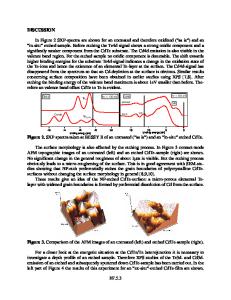
1. Introduction Nanostructure fabrication is interesting for the development of optoelectronic devices, because a large enhancement of several optical properties of low dimensional structures is expected due to quantization effects. On the other hand different studies have shown, that the investigation of intrinsic optical properties of 1- and 0- dimensional structures is limited strongly by effects which arise due to imperfect technology [1-3]. In deep etched structures a very pronounced size dependence of the optical properties results mainly from non radiative transitions at the etched sidewalls, which reduce the quantum efficiency. This effect is characterized by the sidewall recombination velocity S and the formation of an optically inactive "dead" layer. If the structures are fabricated by dry etching, the crystal surface will be degraded within about 10 nm by the impinging ions from the etching plasma and a "dead" layer is formed. The InP/InGaAs-system is particularly interesting for the development of future optoelectronic devices based on low dimensional structures. Regarding non radiative recombination S should be nearly two orders of magnitude smaller than for GaAs-based systems [4,5]. In the present paper we have investigated the luminescence in deep wet etched InGaAs/InP wires. For the sizes of these structures there is no emission wavelength shift due to the reduction of the geometrical width. The quantum efficiency should only be controlled by sidewall recombination. We observe a strong dependence of the effective sidewall recombination on the excitation density, caused by the saturation of non radiative recombination centers. Mat. Res. Soc. Symp. Proc. Vol. 283. 01993 Materials Research Society
822
To study the influence of the sidewall recombination for different geometries, we have compared the quantum efficiency of wires and dots. In earlier studies of Patillon et al. [6] a large enhancement of the emission intensity of dots was observed compared to the emission intensity of wires already at geometrical widths of 100 nm. The enhancement of the quantum efficiency was regarded as an indication for a reduction of t
Data Loading...