Germanium Implantation into Silicon: An Alternate Pre-Amorphization/Rapid Thermal Annealing Procedure for Shallow Juncti
- PDF / 844,972 Bytes
- 6 Pages / 417.6 x 639 pts Page_size
- 87 Downloads / 364 Views
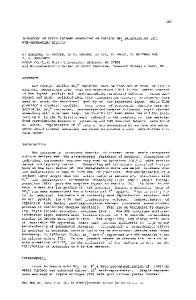
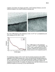
GERMANIUM IMPLANTATION INTO SILICON: AN ALTERNATE PRE-AMORPHIZATIOW RAPID THERMAL ANNEALING PROCEDURE FOR SHALLOW JUNCTION TECHNOILOGY D.K. SADANA*,**, E. MYERS **, J. LIU**, T. FINSTAD***, and G.A. ROZGONYI*,** *Microelectronics Center of North Carolina, Research Triangle Park, NC 27709; **North Carolina State University, Raleigh, NC 27650; ***University of North Carolina, Chapel Hill, NC 27514. ABSTRACT Germanium implantation into Si was conducted to pre-amorphizf thei surface layer prior to a shallow/high dose (42 keY, 2 x 10 cm BF implant. Cross-sectional transmission electron microscopy showed Qt rapid thermal annealing (RTA) of the amorphous layer (without BF 2 ) leaves defect-free material in the implanted region. Only a discrete layer of small (-300A) dislocation loops due to straggling ion damage was found to be present at a depth corresponding to the amorphous/crystalline interface. RTA of the amorphous layer with the BF creatpd a high density of uniformly. distributed fine defect clusteis (-50A) in the surface region (0-500A) in addition to the straggling ion damage. Boron and F profiles obtained by secondary ion mass spectrometry from the unannealed and rapid thermally annealed samples showed the presence of high concentrations of these impurities in the surface region where the fine defect clusters were observed. A comparison of the RTA behavior of the pre-amorphized surface layers (with or without BF 2 ) produced by Ge and self-implantation is presented. INTRODUCTION Control of electric charge in the surface region of modern miniature Si devices is achieved by shallow (
Data Loading...