Pulsed Laser Annealing of Silicon-Germanium Films
- PDF / 3,897,402 Bytes
- 6 Pages / 612 x 792 pts (letter) Page_size
- 83 Downloads / 414 Views
J4.2.1
Pulsed Laser Annealing of Silicon-Germanium Films Sherif Sedky1, Jeremy Schroeder2, Timothy Sands2, Roger Howe3,4 and Tsu-Jae King4 Physics Department, The American University in Cairo, P.O. Box 2511 Cairo, Egypt 2 Department of Materials Science & Engineering, University of California, Berkeley 3 Berkeley Sensor & Actuator Center, University of California, Berkeley 4 Department of Electrical Engineering and Computer Science, University of California, Berkeley
1
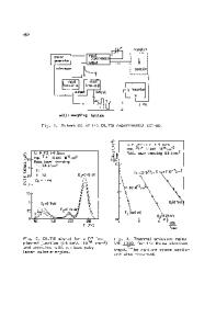
ABSTRACT In this work, we investigate the possibility of using pulsed laser annealing to locally tailor the physical properties of Si1-xGex (18% < x < 90%) prepared by low pressure chemical vapor deposition (LPCVD) at 400°C. Films which were amorphous as deposited showed, after laser annealing, strong {111} texture and a columnar grain microstructure and an average resistivity of 0.7 mΩ.cm. AFM showed that the first few laser pulses result in a noticeable reduction in surface roughness, which is proportional to the pulse energy. However, a large number of successive pulses dramatically increases the surface roughness. INTRODUCTION Over the last decade there has been a tremendous evolution in the field of microelectromechanical systems (MEMS), that mandates their integration monolithically on top of standard, pre-fabricated sense, control and signal processing electronics. This approach is advantageous as it improves system reliability, reduces development costs and shortens time to market. On the other hand, it imposes an upper limit on the MEMS process thermal budget, which is defined by the technology used to fabricate the driving electronics. In spite of the fact that metals [1], amorphous silicon [2], vanadium oxide [3] and sputtered silicon [4] have been used as structural materials for MEMS devices which are post-processed on top of pre-fabricated electronics, each of these materials has its own drawbacks. Metals, with a tendency to creep, such as Al, might result in reliability problems, specifically for RF switches [5]. In addition, the resistivities of metals are slowly varying functions of temperature, which makes them unsuitable for some applications such as high performance infrared focal plane arrays. Amorphous semiconductors have large low frequency (1/f ) noise and high compressive stress that dramatically limit the performance of MEMS devices. Vanadium oxide is not a standard material in IC technology, and it requires special process optimization to obtain the desired activation energy, resistivity and noise. Using a bilayer of a metal and a dielectric [6] can improve reliability but this will be at the cost of process complexity. In general, the performance of a wide variety of MEMS devices is optimized using either polycrystalline silicon or polycrystalline silicon-germanium as a structural layer due to their superior mechanical and thermal properties [7,8], high quality factor [9] and compatibility with standard fabrication processes. The crystallization temperature of silicon can be significantly reduced to 500°C by using Metal
Data Loading...