Growth -Front Modulation in Lamp Zone Melting of Si on SiO 2
- PDF / 1,310,173 Bytes
- 6 Pages / 417.6 x 639 pts Page_size
- 91 Downloads / 281 Views
GROWTH
-FRONT
MODULATION IN LAMP ZONE MELTING OF Si ON SiO2
D. DUTARTRE, D. BENSAHEL, M. HAOND Centre National d'Etudes des T616communications, B.P. 98, 38243, Meylan - Cedex, France
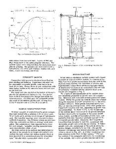
ABSTRACT We present 3 techniques of defect localization we have studied in order to produce Silicon On Insulator films obtained by Lamp Zone Melting. They consist in a periodical variation of the thickness of either the oxide cap, or the polysilicon film, or the underlying oxide layer. We compare the crystallographic quality of the resulting films and in-situ observations of the solidification front for each structure. INTRODUCTION In Zone Melting Recrystallization (ZMR) growth of Silicon On Insulator (SO) films, the crystalline quality of the recrystallized film is related to the solid -liquid interface stability. Contrary to Czochralski growth, in ZMR, the thermal gradients are not easy to control and the crystal quality is very sensitive to any in -plane stress: some crystalline defects remain even at low scan speeds (0.1- 0.2 mm/sec.). These defects are mainly Sub-Grain Boundaries (SGBs) and defect trail /l/. In order to avoid these randomly located defects, different methods which confine the defects to predetermined locations have been experienced. These techniques aim at shaping the solidification front: in laser recrystallization, anti-reflective coating /2/ or heat-sink structures /3/ act via radiation to the film or heat dissipation to the substrate respectively. In the case of lamps or graphite strip -heaters, due to their lower energy densities and thermal gradients, additional mechanisms such as thin film effects related to the interfacial energy may be utilized for the modulation of the solidification front /1,4/. On the other hand, for industrial applications, an entrainment technique has to be contamination -free, efficient and reproducible. In this paper, we present 3 techniques we have tried by patterning either the underlying oxide, or the polysilicon, or the capping oxide. For each structure, the crystalline quality of the SOI film is examined and is discussed in connection with in-situ observations of the solidification front. Finally, the main requirements of an entrainment technique are analyzed. EXPERIMENTAL 4-in., Si wafers are oxidized up to 1 pm. A 0.5 4m thick film of polysilicon is then deposited and capped with a 1.5 pm oxide layer. The defect entrainment is achieved by the modulation of either the polysilicon layer or the underlying or the capping oxide. The pattern consists in parallel, 4 pm wide, 36 pm spaced stripes extending along the wafer. - In the first set of samples (Si relief), the polysilicon is etched into 4 4m wide lines so that its thickness is locally reduced to about 0.3 pm (Fig. la). - In the second set of samples (cap relief), the capping oxide layer is Mat. Res. Soc. Symp. Proc. Vol. 74. c 1987 Materials Research Society
562
etched the same way (Fig. 1b). - In the third set of samples, the underlying oxide layer is thinned within 36 pm wide stripes by using the reverse mask of th
Data Loading...


