Modulation of electron transfer in Si/SiO 2 /HfO 2 /Graphene by the HfO 2 thickness
- PDF / 2,027,157 Bytes
- 9 Pages / 595.276 x 790.866 pts Page_size
- 54 Downloads / 378 Views
Modulation of electron transfer in Si/SiO2/HfO2/Graphene by the HfO2 thickness Y. Ben Maad1 · A. Durnez2 · H. Ajlani1 · A. Madouri2 · M. Oueslati1 · A. Meftah1 Received: 24 June 2020 / Accepted: 20 August 2020 © Springer-Verlag GmbH Germany, part of Springer Nature 2020
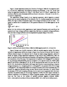
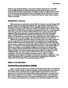
Abstract We studied by Raman spectroscopy the effect of the variation of the thickness of the H fO2 layer in Si/SiO2/HfO2/Graphene heterostructures on the density of carrier transferred to graphene. Three thicknesses of the HfO2 layer equal to 30, 20, and 5 nm were used. Analysis of the behavior of peaks G and 2D as well as the Raman intensity ratios I D/IG and I 2D/IG shows that the density of carriers transferred to graphene increases when the thickness of the H fO2 layer decreases from 30 to 5 nm. Analysis of the photoluminescence (PL) spectra of Si/SiO2/HfO2 structures reveals the presence of bands associated with defects. These are essentially associated with oxygen vacancies in H fO2 and are responsible for the transfer of carriers to the graphene layer. The measured refractive index of H fO2 by ellipsometry shows an increase in the density of the defects in HfO2 with a decrease in its thickness in agreement with Raman results. Keywords Graphene · HfO2 · Raman · Photoluminescence
1 Introduction For several years now, research in microelectronics has focused on the problem of downscaling the components’ geometry to improve their properties while remaining costs effective [1–3]. Nowadays, the study of Si/SiO2/HfO2 heterostructures presents an increasing interest considering their possible applications in various fields such as the development of high k transistors. Indeed, following the evolution of technologies and manufacturing processes and to cope with the miniaturization of electronic components, replacement of the S iO2 layers generally used in the microelectronic industry is necessary. To do this, Hafnium dioxide (HfO2), with its wide band-gap (5.6–5.8 eV) [4, 5] and its high dielectric constant (k = 16–25) [6] seems to be the ideal candidate. The use of HfO2 makes it possible, for example, to avoid the problems of tunnel leakage through various barriers encountered with S iO2 [7, 8]. In terms of capacity, the * H. Ajlani [email protected] 1
Faculty of Sciences of Tunis, Laboratory of Nanomaterials Nanotechnology and Energy (2NE), University of Tunis El Manar, 2092 Tunis, Tunisia
Centre de Nanosciences et de Nanotechnologies C2N, Palaiseau, France
2
use of H fO2 makes it possible to use thicker layers than those of SiO2 while retaining the same capacity value, and consequently, the tunnel leakage is then reduced [9]. Among the other advantages that HfO2 presents, we also note its good compatibility with silicon; it is thermodynamically stable when in contact with it. Also, H fO2 has an energy barrier (1.5 eV for electrons and 3.4 eV for holes) lower than SiO2 ones (3.1 eV for electrons and 4.9 eV for holes) [10]. In the microelectronics industry, graphene occupies a central place thanks to
Data Loading...