Growth of Cu-rich/poor CuInS 2 thin films by the sequential modulated flux deposition technique
- PDF / 1,305,099 Bytes
- 6 Pages / 595 x 842 pts (A4) Page_size
- 24 Downloads / 338 Views
1165-M02-06
Growth of Cu-rich/poor CuInS2 thin films by the sequential modulated flux deposition technique A. Bollero1∗, M. Grossberg2, T. Raadik2, J. F. Trigo1, J. Herrero1 and M. T. Gutiérrez1 1 Dep. of Energy, CIEMAT, Av. Complutense 22, 28040 Madrid, Spain 2 Dep. of Materials Science, Tallinn University of Technology (TUT), Ehitajate tee 5, Tallinn 19086, Estonia ∗
Corresponding author. Tel.: +34 913466364; fax: +34 913466037. E-mail address: [email protected]
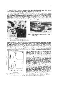
ABSTRACT CuInS2 has emerged during recent years as a good candidate to substitute CuInSe2 as polycrystalline absorber in thin film solar cells, mainly due to its direct band gap energy of 1.5 eV. In this study, absorber layers of both Cu-rich and Cu-poor types have been grown on sodalime glass substrates by proper selection of the deposition parameters. The morphology and the optical properties of the resulting CuInS2 films were studied in dependence of the deposition order of the elemental constituents: alternate evaporation of the precursors, simultaneous deposition of the three constituents and sequential modulation of the evaporation fluxes. INTRODUCTION Thin film polycristalline solar cells have been widely studied during recent years because of the increasing conversion efficiencies achieved. CuInS2 is an excellent candidate to be used as absorber film due to its direct band energy gap Eg ≈ 1.5 eV and its high absorption coefficient (α ~ 104-105 cm-1 for hν>Eg). CuInS2-based solar cells exhibit however lower efficiencies than those based on the ternary analogue CuInSe2. A better understanding of the microstructure and the influence that the preparation parameters have on it will be fundamental to improve the efficiency of CuInS2-based devices. Cu-rich and Cu-poor CuInS2 thin films have been prepared by using different techniques and following different procedures [1]. The use of Cu excess during the preparation leads to CuS binary phases segregated on the film surface which must be removed prior to the deposition of the subsequent layers; this is usually done by applying a toxic KCN etching treatment. This step can be avoided by preparing CuInS2 films with a reduced Cu content. However, the procedure may be rather complex [2]. This work shows the possibility of producing both Cu-rich and Cupoor CuInS2 films by proper choice of the deposition sequence and modulation of the evaporation fluxes. The influence of the microstructure and morphology on the optical properties of the films is studied. EXPERIMENTAL DETAILS CuInS2 films were prepared on soda-lime glass substrates by controlled evaporation of the constituent elements in a self-designed evaporation chamber. The substrate temperature was maintained constant at a relatively low value of 350ºC. In a first stage of the study, films with a thickness of 200-285 nm were prepared following different deposition sequences of In and Cu while keeping a controlled sulphur pressure: 1st In/2nd Cu (CIS-A with 285 nm in thickness); 1st
Cu/2nd In (CIS-B with 230 nm); and In+Cu simultaneously (CIS-C wi
Data Loading...