Growth of CuO and CuGaO 2 Thin Films by Spin-coating Method
- PDF / 260,902 Bytes
- 4 Pages / 432 x 648 pts Page_size
- 29 Downloads / 510 Views
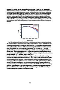
Growth of CuO and CuGaO2 Thin Films by Spin-coating Method Afishah Alias, Masato Sakamoto, and Katsuhiro Uesugi Division of Engineering for Composite Functions, Muroran Institute of Technology, Muroran, Hokkaido 050-8585, Japan ABSTRACT CuO and CuGaO2 thin films have been grown on Si (100) substrates using a sol-gel spincoating method. CuO films were successfully fabricated by the annealing around 700oC. At higher temperatures (>800oC), pyramidal CuO islands with 1~2ȝm in width and 0.4~0.8ȝm in height were observed. They arranged structures as a straight line parallel to the and directions, which suggests the self-organized growth of CuO pyramidal islands. Delafossite CuGaO2 films were fabricated as well, using Cu-Ga-O mixed solutions with Ga/(Cu+Ga) atomic ratio of 0.5. These results indicate that Cu-based compounds were fabricated by the sol-gel spincoating method. INTRODUCTION Transparent conducting oxides (TCOs) have been widely used in optoelectronics areas due to their high optical transparency, low resistivity and wide energy bandgap [1]. TCOs find a wide range of important applications such as light emitting diodes; solar cell and flat panel display [2-4]. However, most of the TCOs such as ZnO and SnO2 have n-type conductivity. In order to fabricate p-n junction devices with the combination of the two types of TCOs, the p-type TCOs is much desired [4]. P-type TCOs would add significant new applications if sufficient conductivity and transparency could be obtained [5]. Recently, p-type Cu-based compounds such as CuMO2 (M=Al, Ga, In) have been widely studied. Ueda et al. have reported that the p-type CuGaO2 films with energy band gap of ~3.6 eV was successfully grown using pulsed laser deposition [2]. The high merit of p-type CuGaO2 has been fabricated by using pulsed laser deposition [2] and radio frequency magnetron sputtering [6]. However, fabrication process of CuGaO2 films using source solution such as sol-gel and spray methods has not been reported yet. Sol gel method is preferable due to its advantages, including the films can be able to produce at a large scale at atmosphere pressure as an addition of a low cost process. In this paper, Cu-Ga-O source solutions were prepared using Copper (II) acetate monohydrate ((CH3COO)2Cu·H2O) and tris acetylacetonato gallium (III) (Ga(C5H7O2)3), and Cu-based thin films were fabricated on Si (100) substrates by a sol-gel spin-coating method. EXPERIMENTAL CuO, GaO and CuGaO2 films were fabricated on Si (100) substrates using Cu-Ga-O source solutions. (CH3COO)2Cu·H2O and Ga(C5H7O2)3 were dissolved in 2-propanol, respectively. Then monoethanolamine (MEA) as a stabilizing agent was added in each of the source solution. Each mixed solution was separately stirred at 50oC for 1 h and the transparent sol solutions for the growth of each CuO and GaO films were formed. A mixture of Ga/Cu with
35
various atomic ratios was used as Cu-Ga-O source solution. The sol solution was spin-coated on Si substrates at 3000 rpm in 15 s. The sol films were pre-baked at 100~300oC under N2
Data Loading...