High Dose Implantation of Nickel into Silicon
- PDF / 1,968,847 Bytes
- 6 Pages / 417.6 x 639 pts Page_size
- 42 Downloads / 350 Views
Mat. Res. Soc. Symp. Proc. Vol. 54. '1986 Materials Research Society
748
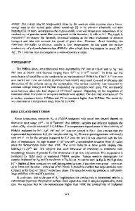
a
b
cd
Figure 1. Scanning electron micrographs showing the effects of 58 Ni+ implantation at 170 keV into silicon for the as implanted and post annealed case. (a) 1.8 x 1018 cm- 2 , as implanted, (b) 6 X 1017 cm- 2 , y5 implanted, (c) 6 X 1017 cm- 2 , 900 0C, 30 min annealing, and (d) 1.5 X 10zl cm- 2, 900 0C, 30 min annealing. infrared pyrometer during implantation. The surface temperature was below the minimum detectable temperature of the pyrometer, 700C. The implantation doses obtained were 0.05, 0.1, 0.5, 1.5, 3, 6, and 18 X 1017 ions cm- 2 . After nickel implantation, sections of each wafer were furnace annealed at 9000C for 30 min in dry nitrogen. RESULTS AND DISCUSSION
A metallic appearance is present on samples with a dose greater than 3 X 10¹⁷ ions cm- . The highest dose had a rough, matte or abraded surface suggesting ion beam sputtering effects. In general, the completely amorphous surface has a metallic-like appigrancg. The metal-lUke surface on samples with a dose greater than 3 X 10" cm- suggests an amorphous surface or a nickel surface layer. Figure 1 contains SEN micrographs of several implanted samples. Figure 1(a) is a sample dose of 1.8 X 1018 cm-2 that was roughened due to ion 2 beam sputtering. For lower dose samples, such as 6 X 10¹⁷ ions cm- , Fig. 1(b), the surface is featu'eless. After annealing in nitrogen at 900 0 C for 30 min, these samples take on a matte or hazy appearance. At doses above 1.5 X 10¹⁷ ions cm- 2 , the surface has a metallic appearance.
749
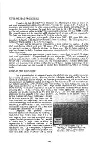
SURFACEI
MIT -2
0.2 pm
a
b
Figure 2. Cross-sectional transmission ele ron 2micrographs for 58 Ni+ (a) 1.5 X 10" cm- dose and (b) 6 X 10¹⁷ implanted in silicon at 170 KeY: cm- 2 dose. Shown in Fig re 1Ic) and (d) are SEM micrographs of samples with doses of 6 and 1.5 X 10"9 cm- , respectively. The matte or hazy appearance is due to the large areas of light and dark islands or patches. Although the area of the light islands increases with dose, it is not clear whether these islands correspond to nickel segregation or to beam damage. Subsequent detailed materials analysis with Rutherford backscatterlng (RBS), spreading resistance profiling (SRP), and cross-sectional transmission microscopy (XTEM) were performed on all the high dose implanted samples. 7 In2 this paper, we have limited our discussion to the 1.5 and 6x101 cm samples because these samples were representative of high dose implantation effects. The 1.5 X 1017 cm- 2 dose corresponds to the surface change from silicon to metallic color between the as-implanted and annealed case. The 6 X 1017 cm- 2 sample had the highest dose that did not exhibit surface degradation due to beam sputtering effects. Shown in Figure 2(a) and (b) are XTEM micrographs of samples with implantation doses of 1.5 and 6 X 1017 cm- 2 , respectively. For the 2 1.5 X 1017 cm- dose, Figure 2(a), a band of clusters centered around Rp was observ.J within a continuous amorphous layer extending from the surface. The amorphous/c