High Performance High Dielectric Constant Films Deposited by Dual Spectral Source Rapid Isothermal Assisted Metalorganic
- PDF / 262,318 Bytes
- 6 Pages / 414.72 x 648 pts Page_size
- 44 Downloads / 318 Views
ABSTRACT Dual spectral source assisted MOCVD is an ideal technique for the deposition of high dielectric constant materials as well as other electronic and optical materials. Tungsten halogen lamps and a deuterium lamp are used as the sources of optical and thermal energy. Ta20 5 films were deposited at 200'C for 30 minutes and annealed at 600'C for 30 minutes have shown leakage current densities as low as 1010 Al cm2 for gate voltage under 5V. To the best of our knowledge, these are the best results reported to date by other researchers. The high energy photons used in the in-situ cleaning and deposition process play an important role in obtaining high quality films of Ta2O5 . I. INTRODUCTION
For the development of next generation of Si ICs, there is a need for the development of high dielectric constant materials that can be used as the gate dielectric material as well as the dielectric of the DRAM capacitor. From the device performance and reliability point of view, the high dielectric materials used in future Si ICs must meet several requirements. Any new material must show low leakage current and high dielectric constant values. The process should provide materials with low microscopic defects, low thermal and residual stress. Additionally, low processing temperatures must be used in the deposition of the new dielectric materials. A number of high dielectric materials have been investigated throughout the world [1,2]. Ta20 5 films deposited by chemical vapor deposition (CVD) techniques are promising candidates (the bulk dielectric constant of Ta20 5 is 25). However, because leakage current densities in Ta20 5 are higher than those in conventional dielectrics such as silicon nitrides or silicon dioxides, it is difficult to use these materials for Si IC applications. In this paper, we report the results of Ta205 films with low leakage currents deposited by dual spectral source rapid isothermal processing (DSSRIP) assisted metalorganic chemical vapor deposition (MOCVD) on Si and conducting
133 0 Mat. Res. Soc. Symp. Proc. Vol. 470 1997 Materials Research Society
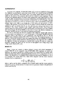
materials. In addition to the electrical characterization, the results of structural characterization and thermal stress measurements are also reported. II.EXPERIMENTAL Rapid isothermal processing based on incoherent radiation as the source of optical and thermal energy is emerging as a key low thermal budget processing technique. Both for CVD and other applications, the use of high energy photons (wavelength less than 800nm ) in the RIP systems provides superior material and device properties than the RIP systems which do not use high energy photons. noo -
Deposited at 4009C for 15 mins,
-
Deposited at 200 C for 30 mins.
Fig. I. Complete
1oo0
thermal cycle showing in-situ cleaning,
deposition and annealing of Ta,0 5 films.
500
o•;
V400
'-..........................
"300 200 -
100
0
10
20
30
40 50 Time (Minute)
60
70
80
90
Ta,0 5 films were deposited on p-type (100) wafers and poly-Si substrate with a thin layer of Si3N4. The sub
Data Loading...