High Quality Oxide Films Deposited at Room Temperature by Ion Beam Sputtering
- PDF / 545,306 Bytes
- 6 Pages / 432 x 648 pts Page_size
- 17 Downloads / 372 Views
MRS Advances © 2018 Materials Research Society DOI: 10.1557/adv.2018.157
High Quality Oxide Films Deposited at Room Temperature by Ion Beam Sputtering Gerard E. Henein1, Juraj Topolancik2 and Kerry Siebein1 1 Center for Nanoscale Science and Technology, National Institute of Standards and Technology, Gaithersburg, MD 20899
2
Roche Sequencing Solutions, 4155 Hopyard Dr., Suite 200, Pleasanton, CA 94588
ABSTRACT
We have deposited dense and pinhole-free thin films of SiO2, Al2O3 and ITO at room temperature via ion beam sputtering. The SiO2 films were found to be of similar quality as thermal oxide with a resistivity greater than 1015 Ω·cm and breakdown field in excess of 7 MV/cm. The Al2O3 films were part of a Pt- Al2O3-Pt vertical tunnel junction and were kept extremely thin, from 2 nm to 4 nm. The current-voltage characteristics of these junctions indicated a breakdown field in excess of 20 MV/cm, roughly twice that achieved by ALD films. This breakdown voltage was found to be independent of junction area, strongly suggesting the absence of pinholes in the film. The ITO films were 50 nm to 100 nm thick. As deposited, they are fully transparent with an electrical resistivity of 5x10⁻⁴ Ω·cm.
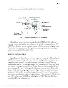
INTRODUCTION The highest quality oxides such as SiO2, Al2O3 and Indium Tin Oxide (ITO) require high temperature processing either during the growth of the film or annealing post-growth. Thermal SiO2 is grown at ≈1000 °C [1], ALD Al2O3 is deposited at ≈300 °C [2], and magnetron-sputtered ITO must be annealed above 350 °C in order to turn the film conductive [3]. These elevated temperature requirements are not compatible with polymer substrates used for flexible electronics. Our objective was to explore ion beam deposition as an alternative room temperature technique and characterize the film properties. FILM DEPOSITION TECHNIQUE The films of SiO2, Al2O3 and ITO were deposited on silicon wafers at room temperature via ion beam sputtering as depicted in figure 1. The deposition system consists of a 3-grid 14 cm RF ion gun directed at 200 mm targets of SiO 2, Al and ITO. All three processes require a small flow of O2 to achieve stoichiometry. Typical conditions were: argon flow rate 3.3x10 -7 m3/s (20 sccm), beam voltage 600 V, beam
219
Downloaded from https://www.cambridge.org/core. University of Pennsylvania Libraries, on 13 May 2018 at 23:39:45, subject to the Cambridge Core terms of use, available at https://www.cambridge.org/core/terms. https://doi.org/10.1557/adv.2018.157
current 220 mA and acceleration voltage 150 V. The substrate wafers rotated at 10 rpm and were kept at 20 °C. The base vacuum prior to deposition was 2.6x10 -6 Pa (1.5 x10⁻⁸ Torr).
Figure 1. Schematics of the ion beam deposition system
MEASUREMENT TECHNIQUES The measurements techniques consisted of current-voltage, ellipsometry, chemical etching and X-ray diffraction (XRD). We used a mercury probe directly on the oxide wafers, and a standard probe station on the devices, to measure resistivity, breakdown voltage and detect pinholes. Ellipsometry yie
Data Loading...


