High-Rate Deposition of Intrinsic a-Si:H and pc-Si:H Layers for Thin-Film Silicon Solar Cells using a Dynamic Deposition
- PDF / 622,312 Bytes
- 6 Pages / 432 x 648 pts Page_size
- 30 Downloads / 253 Views
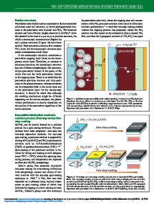
High-Rate Deposition of Intrinsic a-Si:H and μc-Si:H Layers for Thin-Film Silicon Solar Cells using a Dynamic Deposition Process T. Zimmermann1,4, A. J. Flikweert1, T. Merdzhanova1, J. Woerdenweber1, A. Gordijn1, K. Dybek2, F. Stahr3 and J. W. Bartha4 1 IEK5-Photovoltaik, Forschungszentrum Jülich, D-52425 Jülich, Germany 2 Von Ardenne Anlagentechnik GmbH, Am Hahnweg 16, D-01328 Weissig, Germany 3 Forschungs- und Applikationslabor Plasmatechnik GmbH, Gostritzer Str. 67, D-01217 Dresden, Germany 4 Technische Universität Dresden, Fakultät Elektrotechnik und Informationstechnik, Institut für Halbleiter- und Mikrosystemtechnik, D-01062 Dresden, Germany ABSTRACT Thin-film silicon solar cells based on hydrogenated amorphous silicon (a-Si:H) and hydrogenated microcrystalline silicon (μc-Si:H) absorber layers are typically deposited using static plasma-enhanced chemical vapor deposition (PECVD) processes. It has been found that the use of very-high frequencies (VHF) is beneficial for the material quality at high deposition rates when compared to radio-frequency (RF) processes. In the present work a dynamic VHF-PECVD technique using linear plasma sources is developed. The linear plasma sources facilitate the use of very-high excitation frequencies on large electrode areas without compromising on the homogeneity of the deposition process. It is shown that state-of-the-art a-Si:H and μc-Si:H single-junction solar cells can be deposited incorporating intrinsic layers grown dynamically by VHF-PECVD at 0.35 nm/s and 0.95 nm/s, respectively. INTRODUCTION Thin-film silicon tandem solar cells based on hydrogenated amorphous silicon (a-Si:H) and hydrogenated microcrystalline silicon (μc-Si:H) absorber layers are a very promising photovoltaic technology. The material combination is ideally suited for the solar spectrum, there is no shortage of the absorber material and it is environmentally benign. The a-Si:H and μc-Si:H layers are conventionally deposited statically by plasmaenhanced chemical vapor deposition (PECVD) processes. It has been found that the application of very-high frequencies (VHF) is beneficial for the material quality at high growth rates when compared to radio-frequency (RF) PECVD processes [1–6]. However, very-high excitation frequencies typically lead to an inhomogeneous voltage distribution on large electrodes due to the standing wave effect. As a result, the material growth is not uniform. In the present work a scalable dynamic VHF-PECVD technique is developed. Linear plasma sources are used which are scaled up in only one electrode dimension instead of both dimensions as for planar electrodes [7]. The number of power feeds to the linear plasma source is adapted to its length and the excitation frequency in order to ensure a homogeneous deposition along the length of the electrode. The uniformity of the deposition process in the second substrate dimension is facilitated by moving the substrate in front of and parallel to the electrode at a constant speed [7]. The constant speed ensures that every point on the sub
Data Loading...