High Deposition Rate Amorphous Silicon Solar Cells and Thin Film Transistors Using the Pulsed Plasma Pecvd Technique
- PDF / 415,260 Bytes
- 6 Pages / 414.72 x 648 pts Page_size
- 35 Downloads / 320 Views
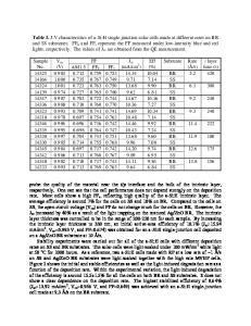
Scott Morrison, Jianping Xi, Arun Madan MVSystems Inc., 327 Lamb Lane, Golden, Colorado 80401, or 17301 W. Colfax Ave., Suite 305, Golden, CO 80401, USA ABSTRACT The pulsed plasma technique has been shown to increase the deposition rate without an increase in the particulate count in the plasma which is an important factor determining the yield of commercial products such as active matrix displays. In this paper, we report the deposition of amorphous silicon at deposition rates of up to 15 A/sec. using a modulation frequency in the range of 1-100kHz. These materials have been incorporated into a simple p/i/n solar cell and thin film transistor (TFT) configurations. We report on the effect of the conversion efficiency as a function of the modulation frequency, which in turn is related to the deposition rate. We also report on the TFT performance with modulation frequency and compare the results with devices made under the conventional continuous wave PECVD plasma at 13.56MHz. INTRODUCTION State of the art a-S:H films are normally deposited at the rate of 1-3 A/sec using the PECVD technique employing a capacitively coupled multi-chamber system operating at a fixed continuous frequency of 13.56MHz. In this technique, increasing the deposition rate by merely raising the power generally leads to dust formation and deterioration in the opto-electronic properties of the material; other techniques have been investigated to circumvent this problem, such as by the use of higher excitation frequency which can lead to deposition rates in excess of 10A/s and still lead to relatively good properties of the films [1]. A technique that we consider, in this paper, uses instead a pulsed PECVD technique as this can, in addition to increasing the deposition rate, can suppress dust formation, a prerequisite in obtaining high yields in production. [2]. This is accomplished by modulating the plasma in the range up to 100kHz with an ON-time to OFF-time ratio of 10-50%, so that negatively charged particles can be extracted before they grow to sizes that can cause manufacturing yield problems. The time averaged plasma properties when so modulated also differ markedly from those generated using continuous wave (CW) excitation. Because the discharge in the plasma is not in equilibrium, time modulation permits tuning of processing conditions, often for the better. EXPERIMENTAL DETAILS
Amorphous silicon (a-Si) films were produced in a commercially available PECVD system specifically designed for the thin film semiconductor market and manufactured by MVSystems, Inc. The samples were prepared on a 10 cm X 10 cm substrate situated on the anode side of the RF electrode assembly. The pulsing (variation between 0-100kHz, on/off ratio of 50%) was superimposed onto a 13.56 MHz signal applied to the RF plate. Generally the power used was in the range of 3-35 Watts, fixed anode- cathode distance up to 3cms, a flow rate of silane up to 100 sccm, the deposition pressure up to 650 mTorr and the temperature of the substrate up to 230 deg. C. The a-Si sample
Data Loading...