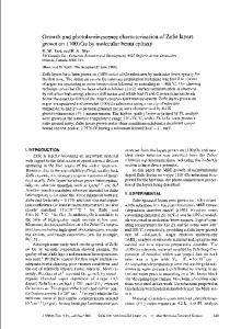
Homoepitaxial Growth of p-Type ZnSe Layers on Dry-Etched Substrates
- PDF / 236,820 Bytes
- 6 Pages / 420.48 x 639 pts Page_size
- 80 Downloads / 287 Views
GROWTH
HOMOEPITAXIAL
OF
p-TYPE
ZnSe
LAYERS
ON
DRY-ETCHED
SUBSTRATES K. Ohkawa
and
T. Mitsuyu
Central Research Laboratories, Matsushita Electric Ind. Co., Ltd Moriguchi, Osaka 570, Japan
ABSTRACT We
have
succeeded
in
the
growth
of
p-type
homoepitaxial
ZnSe
layers. The layers have been grown by molecular beam epitaxy (MBE) on (100) ZnSe substrates dry-etched with BCI 3 plasma to eliminate polishing damage. Nitrogen acceptors were incorporated by nitrogen radical doping during MBE growth. Hall measurement by using Pt electrodes have indicated
that
the
N-doped ZnSe
homoepitaxial
layers are
p-type
with
3
hole concentration of 8.9x1015 cm- . 12-K photoluminescence (PL) from the layers exhibited strong neutral-acceptor-bound exciton emission (1 1) at 2.7931 eV, indicating the peak energy of 11 emission from the typical
strain-free ZnSe:N.
INTRODUCTION ZnSe is a promising material for efficient blue light-emitting devices due to its direct bandgap of 2.7 eV at room temperature. The efficient devices
are not
p-type ZnSe.
realized for
To date, there
conduction in ZnSe [1-6]. measurements. substrates were
The
there are two
problem
used
in achieving
have been a number
However,
first
usually
the difficulties
is
for the
the
of reports
of p-type
problems in the electrical
influence
epitaxial
low-resistivity
growth
of
substrates.
of ZnSe,
GaAs
because
of
a small lattice mismatch. In this case there is a possibility of measuring p-type GaAs:Zn
in the
ZnSe/GaAs
heterointerface
by
Zn
diffusion
into
GaAs substrate. The second possibility has been pointed out by Neumark that twinnings are conductive to giving p-type behavior [7]. Therefore we consider that p-type conduction
in ZnSe homoepitaxial
layers is the best
evidence of achieving p-type ZnSe.
Mat. Res. Soc. Symp. Proc. Vol. 228. ',1992 Materials Research Society
308
TREATMENT OF ZnSe SUBSTRATES FOR HOMOEPITAXY ZnSe single-crystal Laboratory
substrates obtained
from Eagle-Picher
highly resistive
were (100) oriented,
and free from
As-polished substrates have polishing damage on the surface. the polishing damage
for homoepitaxy.
is necessary
Research twinning.
Removal of
We have found that
dry etching technique provide high-quality surface of ZnSe substrates for homoepitaxy [8]. After cleaning in organic solvents, the as-polished plasma with pressure of 60 mTorr
substrates were etched in a BCI 3 about
1 W/cm 2 of radio-frequency
dry-etched
by
about
10 PIm
were thermally etched
(RF) power
in depth.
Prior
at 600 °C for
density. The
to growth,
the
substrates ZnSe
at
were
substrates
10 min under ultrahigh vacuum
of
molecular beam epitaxy (MBE) chamber.
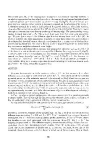
'-.
Co Z LU
IZ -J.
440---450
500
550
600
WAVELENGTH (nm) FIG.I.
12-K photoluminescence
etched ZnSe substrates. (440-450 nm) is magnified.
spectra
Horizontal
from (a)
scale
for
as-polished excitonic
and (b) dry-
emission
region
309
Photoluminescence the
ZnSe
dry-etched
(PL)
from
spectra obtained
subst
Data Loading...