Hot-Wire Chemical Vapor Deposition Epitaxy on Polycrystalline Silicon Seeds on Glass
- PDF / 417,827 Bytes
- 5 Pages / 612 x 792 pts (letter) Page_size
- 66 Downloads / 319 Views
0989-A06-16
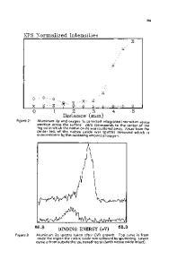
Hot-Wire Chemical Vapor Deposition Epitaxy on Polycrystalline Silicon Seeds on Glass Charles W. Teplin1, Howard M. Branz1, Kim M. Jones1, Manuel J. Romero1, Paul Stradins1, and Stefan Gall2 1 NCPV, NREL, 1617 Cole Blvd, Golden, CO, 80401 2 Hahn-Meitner-Institut Berlin, KekulÈstr. 5, D-12489, Berlin, Germany ABSTRACT During the last few years, hot-wire chemical vapor deposition (HWCVD) has been explored as a low-temperature process for epitaxially thickening c-Si seeds layers on low cost substrates. Here, we demonstrate HWCVD epitaxy on thin polycrystalline silicon seed layers on borosilicate glass substrates. The crystal Si seeds are large-grained (~10 µm) polycrystalline silicon that were fabricated by Al-induced crystallization of a-Si. We report the growth of 0.5 µm of epitaxy at ~670∞C. INTRODUCTION The high cost of the crystal silicon (c-Si) wafers in wafer-based photovoltaics has motivated recent research into cheaper forms of c-Si [1-4]. Numerous approaches have been explored to achieve c-Si of adequate quality to fabricate efficient solar cells. Perhaps the simplest approach has been to simply crystallize a-Si films on glass by annealing after deposition (solid phase crystallization ñ or SPC). Using SPC, mini-module efficiencies of up to 9.8% have been achieved [5]. However, SPC results in a log-normal distribution of Si grain sizes with many small grains and the largest grain size of about 1 micron [6]. The boundaries between these grains affect the electrical properties of the material. Reducing or eliminating these grain boundaries could dramatically improve the carrier lifetimes in this material and increase the achievable photovoltaic efficiency. One approach to reduce the density of grain boundaries is to carefully control the crystallization process using Al-induced crystallization (AIC) of a-Si [7]. This process yields dramatically larger grains. However, film thicknesses are limited and the Al doping level is too high for the Si to act as an effective photovoltaic absorber. Thus, a second step ñ in which the AIC seed layers are epitaxially thickened ñ is required. The initial devices based on Al induced crystallization of a-Si have shown promising open circuit voltages [7, 8]. Epitaxy on AIC seed layers has been achieved using electron cyclotron resonance CVD (ECR-CVD) [7, 9], ion beam assisted deposition (IAD) [10], and electron-beam evaporation [11]. We have explored the use of hot-wire chemical vapor deposition (HWCVD) for the epitaxy step at substrate temperatures above 600∞C, because HWCVD appears straightforward to scale for large-scale production and because we recently demonstrated the possibility of thick epitaxy (at least 11 µm) at high growth rates (>100 nm/min) using HWCVD on (100) Si wafers [12]. Previously, Stradal and coworkers explored HWCVD epitaxy on poly-Si seed layers below 500∞C and found only limited epitaxial thicknesses (
Data Loading...