Hydrogen Etching Effects During Plasma Doping Processes and Impact on Shallow Junction Formation
- PDF / 344,149 Bytes
- 6 Pages / 414.72 x 648 pts Page_size
- 28 Downloads / 282 Views
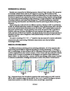
microwave source, vacuum and gas handling, temperature control, and high voltage pulse generator. The details of the MMB plasma system were described elsewhere [2]. The applied microwave power was 730 watts and the working pressure was 50 mT. Measured by a Langmuir probe, typical equilibrium hydrogen plasma parameters for these experiments were: ion density ni ; 2.5x 10¹⁰ /cm 3, electron temperature T. - 4.5 eV, and plasma potential Vp t 20 V. The PII process conditions are: pulse voltage V = 0 to -6 kV, pulse width txp = 5 to 10 Psec, and pulse repetition frequency prf = 0 to 4 kHz. The substrate temperature was held constant between room temperature and 350 'C, depending on the experiments. The investigation of hydrogen etching rates for single crystalline silicon and SiO 2 began with n-type silicon wafers (, p m 2-6 Q)-cm) which were masked by a patterned Si0 2 structure. In order to investigate the hydrogen etching rates of polycrystalline silicon and aluminum, a 1000 A undoped poly-Si film was deposited on a silicon substrate by plasma enhanced chemical vapor deposition (PECVD) at 650 'C. A 2000 A aluminum film was deposited on the poly-Si surface and patterned as a mask. The patterned wafers then underwent hydrogen PII for 30 minutes. The hydrogen etching rate of Si0 2 was determined by optical reflection measurements of the oxide layer thickness before and after the process. The etching depths of the unmasked silicon and polySi were measured with a Dektak profilometer after the masks were removed. The etching depth of aluminum was also determined by a Dektak profilometer with adjustments for the original aluminum film thickness and the poly-Si removed by etching. A photoresist (PR) masked silicon wafer was prepared for etching rate measurements of PR films. Photoresist films were chosen for the experiments due to its potential for use as a doping mask. A positive photoresist (S-1827) film was patterned on a silicon wafer by a standard lithography procedure. The initial thickness of PR film after a 30 min hardbake at 125 *C was -2.8 tim. The etching depth of the photoresist film was also determined with a Dektak profilometer. RESULTS AND DISCUSSION Fig. 1 shows etching rates of silicon, poly-Si, and Si0 2 materials versus substrate temperature when the samples were immersed in hydrogen plasma without the high voltage pulses. The etching rates are less than 5 A/min for all materials, independent of substrate temperature. Fig. 2 shows the hydrogen PII etching rates of silicon, poly-Si, and Si0 2 versus substrate temperature with -6 kV pulses, 5 ýtsec pulse width and 4 kHz pulse repetition frequency. When the high voltage pulses are applied to the samples, etching rates are increased dramatically and become dependent on substrate temperature. Figs. 3 shows the etching rates of silicon, poly-Si and Si0 2 versus pulse potential when the substrate temperature is 200 *C. The pulse width is 5 psec and the pulse repetition frequency is 4 kHz. When the substrate temperature is increased, higher etching rates and a gre
Data Loading...