Thermally Stable Schottky Contacts to n-GaN
- PDF / 343,603 Bytes
- 5 Pages / 414.72 x 648 pts Page_size
- 34 Downloads / 363 Views
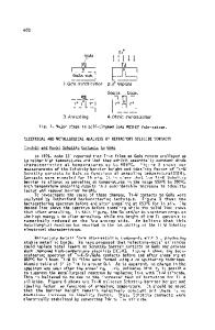
the sample and large area TiN ohmic contacts were formed by rapid thermal annealing at 800 "C for 1 min in nitrogen. Conventional photolithography was then used to pattern the rest of the sample. The samples were etched in 1:1 HCI:DI and were left to pump overnight in the deposition chamber. Re (700 A) and Ni (600 A) contacts were deposited by sputtering. Ni-Ga contacts (approximately
84 at% Ni, 16 at% Ga) were formed by depositing a multilayer of Ni(150 A)/Ga(150 A)/Ni( 26 7 A)
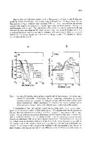
by e-beam evaporation. Schottky metal deposition was followed by lift-off. The Ni/Ga/Ni multilayer was subsequently annealed for 10 min at 400 "C in nitrogen. The diameter of the Schottky dots was 200 jgm. Each sample was patterned with 28 Schottky dots. The Schottky diodes were sequentially annealed at various temperatures from 300 'C-900 "C in an AG 610 rapid thermal annealing furnace (RTA) in a flowing nitrogen atmosphere. After each anneal, I-V measurements were conducted with a Keithley 236 source measure unit to determine the barrier height and the ideality factor of the diodes. I-V measurements were conducted in air at 150 "C. C-V measurements of the as-deposited and annealed diodes were conducted in the parallel mode at room temperature with a Keithley 590 CV analyzer. The capacitance was measured by applying a dc sweep between -5 and 0 V with a 20 mV RMS testing signal at 1 MHz. For each annealing condition, measurements were made on 6-12 diodes. RESULTS AND DISCUSSION I-V measurements I-V measurements were made for the Schottky contacts as a function of annealing temperature. All measurements were carried out at 150 *C. The reverse leakage current varied linearly with bias, which indicates a leakage path in parallel with the Schottky barrier. This behavior was first observed by Chen et al. [11] who suggested that the leakage was probably via threading dislocations. From the reverse bias characteristics, the leakage resistance (Rp) was measured. Once Rp was known, the total forward current (I) was then corrected for the leakage current (Ip) and the resulting current was labeled the diode current (Id). The diode characteristics were then analyzed using the equation [12]: (1) Id = Io exp(q--d )(I- exp(- q2 d)), nkT kT where Vd is the voltage across the diode (Vd = V- IdR), R is the series resistance, n is the ideality factor, and Io is the saturation current. The series resistance, R, was deduced from the Id-V plots using the small signal conductance method [13]. It can be shown that a plot of G/ld vs. G (G = dId/dV) yields a straight line with x-axis intercept 1/R. Once R was deduced, the applied voltage,
V, was corrected for the series voltage drop, IdR. From Equation (1), In(
Id/k)vs.
a plot of
Vd yields In Io as the intercept and q/nkT as the slope. Once Io was
determined, the barrier height (O(I-V)) was determined. C-V measurements C-V measurements of the Schottky diodes were also conducted as a function of annealing temperature. From a linear fit of (1/C2) vs. V, the flat band voltage (Vbi) and the donor concentration (N
Data Loading...


