Interface States at Au/GaAs Schottky Contacts
- PDF / 371,559 Bytes
- 6 Pages / 420.48 x 639 pts Page_size
- 18 Downloads / 355 Views
J.WERNER!)* AND K.PLOOG IIIBM T.J.Watson Research Center, P.O.Box 218, Yorktown Heights, NY 10598, USA 2)Max-Planck-Institut fur Festkorperforschung, Heisenbergstr.l, D-7000 Stuttgart 80, West Germany ABSTRACT We present a new method for the characterization of traps at the interfacial layer of metal/semiconductor contacts. The method is based on measurements of the ac-admittance of Schottky contacts over a wide frequency range. The frequency dependence is analyzed within a new Trap Transistor Model which explains the ac-behavior as well as the dc-characteristics. In particular we propose that the accurrent across the interface consists of capacitive as well as of conductive parts. We are able to deduce the density of trap states at the majority carrier Fermi level as well as the capture cross section of the traps. The model is applied to Au/GaAs-Schottky contacts. We find a weak energy dependence for the density of interface states as well as for their capture cross section within the energy range of 0.45eV to 0.57eV below the conduction band edge. INTRODUCTION The electrical properties of one of the most simple semiconductor devices, the metal-semiconductor contact, are still not well understood. First experiments at these structures were carried out by Braun [ I ] and Schottky 12] explained their rectifying properties in terms of the work functions of the metal, FDm, and the electronegativity of semiconductor, X . Within this theory the Schottky barrier I is given by: y-
=
OmF-
(i)
X
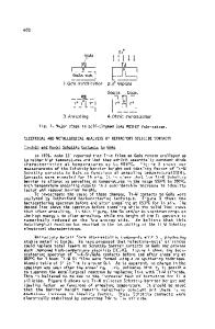
Unfortunately, the barrier 5' that is found from electrical measurements at most Schottky contacts does not obey this simple relationship. This deviation from the ideal behavior is usually attributed to interface states and an interfacial dipole A between the metal and the semiconductor as shown in Fig. 1. The interface states arc capable of capturing free carriers from the semiconductor, becoming electrically charged, and thereby creating a barrier that - for electrostatic reasons - is not given by Eq.( I) but by: E
=
(b, -
X -
A
(2)
The present contribution briefly reports preliminary results of a new electrical method for the analysis of the energy distribution of such interface states. This distribution is obtained from the evaluation of the resonant response of the semiconductor's band bending when the interface states are subjected to a periodical excitation by a small applied ac-voltage. The present analysis is a modification of a model that has successfully been applied to describe the current across grain boundary interfaces [3]. Here the method is exemplified by measturements taken from Au/GaAs-Schottky contacts because this interface is characterized by a pronounced interfacial layer due to oxidation and/or interdiffusion [4,5]. CURRENT TRANSPORT AND BAND BENDING We use a Richardson-Dushman equation to describe the current j, at bias voltage U flowing through the Schottky contact with an interfacial layer as shown in Fig. I. jA1 = 0 AxT2 exp( -Z/kT) {exp(eU/kT) - 11
(3)
Here A' is an effective Richardson cons
Data Loading...


