Improved Characteristics of InGaN Multi-Quantum-Well Laser Diodes Grown on Laterally Epitaxially Overgrown GaN on Sapphi
- PDF / 80,122 Bytes
- 6 Pages / 612 x 792 pts (letter) Page_size
- 99 Downloads / 335 Views
3
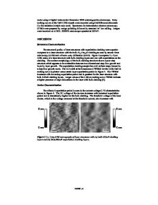
(w) to height (h). This ratio is directly dependent on growth conditions (e.g. V/III ratio, temperature) and “fill factor” (the ratio of open width to pattern period); as w/h increases, wing tilt increases [17,18]. Minimizing wing tilt, minimizes tilt boundary formation and its associated dislocation density at the coalescence fronts. The coalescence of the stripes must be carefully controlled to prevent dislocations from forming at the coalescence fronts to allow a larger area of reduced dislocation density for device placement. EXPERIMENTAL DETAILS In this study, laser diodes were fabricated on high quality fully-coalesced LEO GaN leading to improved device performance. Lasers fabricated on the LEO wings, along with coalescence fronts containing few or no threading dislocations, exhibit a reduced threshold current density compared to those grown on conventional planar GaN on sapphire. The internal quantum efficiency increased from 3% to 22%. InGaN multiple-quantum-well (MQW) laser diodes were grown by MOCVD in a two-flow horizontal reactor at both atmospheric and low pressure. In preparation for patterning a subsequent regrowth, a 2 µm thick GaN seed layer was grown on a c-plane sapphire substrate. A 2000 Å SiO2 mask was patterned into stripes, oriented in the < 1 1 00 >GaN direction, defining a 5 µm mask opening with a periodicity of 20 µm. After ~ 6 µm of LEO GaN growth on the SiO2 mask, the GaN stripes grew laterally and coalesced, forming a flat surface. The conditions for growth and coalescence of the LEO GaN are described elsewhere [18]. Next, the InGaN MQW laser structure was grown on both LEO GaN and on 2 µm GaN on sapphire. The structure had an active region consisting of a 3 period In0.13Ga0.87N (40 Å) /In0.04Ga0.96N:Si (85 Å) MQW followed by a 200 Å Al0.2Ga0.8N:Mg cap. The n and p-type cladding regions surrounding the active region consisted of 25 Å Al0.2Ga0.8N / 25 Å GaN superlattices with a total thickness of 0.45 µm. The cladding regions were Si-doped for the n-cladding and Mg-doped for the p-cladding. A 0.1 µm GaN:Mg layer was used as a contact layer and a 0.1 µm In0.05Ga0.95N:Si layer was used beneath the lower n-type cladding as a compliance layer. Laser diodes were fabricated above the SiO2 mask in the nearly dislocation-free wing regions, above the coalescence fronts of the LEO GaN stripes, as well as above the dislocated window (seed) region. The laser cavity was oriented parallel to the direction of the SiO2 stripes. Laser facets were formed by Cl2 reactive ion etching (RIE) of 45 µm wide mesas of various lengths ranging from 400 µm to 1600 µm and p-contact stripes were patterned on these mesas with widths ranging from 5 µm to 15 µm. The structure was etched around the p-contact stripe through the p-cladding for index guiding. The n and p-contacts were formed by electron beam evaporation of Ti/Al and Pd/Au, respectively. Electrical testing was performed using 50 ns pulses with a 1 kHz pulse repetition rate. RESULTS Figure 1 shows cross-section TEM micrographs of the coalescence region. Ther
Data Loading...