Improving Silicon Crystallinity by Grain Reorientation Annealing
- PDF / 1,962,378 Bytes
- 6 Pages / 612 x 792 pts (letter) Page_size
- 46 Downloads / 396 Views
1153-A05-09
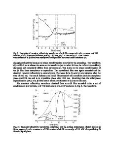
Improving Silicon Crystallinity by Grain Reorientation Annealing K.L. Saenger, J.P. de Souza, D. Inns, K.E. Fogel, and D.K. Sadana IBM Semiconductor Research and Development Center Research Division, T. J. Watson Research Center, Yorktown Heights, NY 10598 ABSTRACT Demand for high efficiency, low-cost solar cells has led to strong interest in postdeposition processing techniques that can improve the crystallinity of thick (1 to 40 µm) silicon films deposited at high growth rates. Here we describe a high temperature grain reorientation annealing process that enables the conversion of polycrystalline silicon (poly-Si) into a single crystal material having the orientation of an underlying single crystal Si seed layer. Poly-Si films of thickness 0.5 to 1.0 µm were deposited by low pressure chemical vapor deposition (LPCVD) on substrates comprising a surface thermal oxide or a 100-oriented single crystal silicon-oninsulator (SOI) layer. After annealing at 1300 oC for 1 hour, poly-Si on oxide shows very significant grain growth, as expected. In contrast, the poly-Si deposited on SOI showed no grain boundaries after annealing, transforming into a single crystal material with a fairly high density of stacking faults. Possible uses and drawbacks of this approach for solar cell applications will be discussed. INTRODUCTION Cost-effective methods for forming thick (1 to 40 µm) layers of single crystal silicon are of interest for applications that include both high efficiency solar cells and thick silicon-oninsulator (SOI) substrates for high power device applications. However, existing growth methods have potential drawbacks [1]. Epitaxial growth on single crystal Si (c-Si) seed layers, typically performed at 800-900 oC, is relatively slow and expensive, and requires careful cleaning of the initial Si substrate surface to ensure good epitaxy. High temperature (~1100 oC) chemical vapor deposition (CVD) processes that can deposit epitaxial Si at a rate of 1 µm/min (for example, atmospheric pressure iodine vapor transport (APIVT) processes) offer promise, but are less well established. Methods utilizing physical vapor deposition of amorphous Si (a-Si) followed by solid phase epitaxy (SPE) at temperatures in the range 550-600 oC are potentially low cost, but share the disadvantage of requiring a clean c-Si/a-Si interface for good epitaxy and present the additional concern that the crystallization of very thick a-Si layers will proceed by a combination of the SPE and undesired spontaneous, randomly nucleated crystallization to form poly-Si. Processes for the bonding and transfer of thick c-Si layers have drawbacks as well: donor wafer bonding to a handle wafer followed by donor wafer etchback sacrifices the entire donor wafer, and the hydrogen ion implantation processes used for SmartCutTM-type splittings are typically restricted to relatively shallow depths (a few hundred nm at most). In this paper we investigate the possibility of creating thick single crystal Si layers by performing a grain reorientation anneal on a
Data Loading...