Solid Phase Epitaxy Process of Ar-Ion Bombarded Silicon Surfaces and Recovery of Crystallinity by Thermal Annealing Obse
- PDF / 4,421,454 Bytes
- 5 Pages / 414.72 x 648 pts Page_size
- 103 Downloads / 274 Views
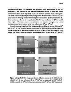
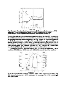
thermal annealing of the specimen was performed at 245-500 0C in the STM chamber under UHV. The specimen was heated by direct heating and its temperature was measured using an optical pyrometer. Dynamic STM observations were performed in a constant tunneling current mode at elevated temperatures. A tip used was a tungsten wire sharpened by electrochemical etching. Results and Discussion As-bombarded Si(001) surfaces are covered with granular grains. Figure 1 shows a typical topographic STM image of the surface at a dose of 1.9xi1 4 cm2 . As bombarded surfaces show essentially the same features within the range of dose examined. The size of the grain is 0.63-1.6 nm in diameter and its density is about 2x10i 5 grains/cm2 . Most of the grains showed bright contrast independent of the sample bias polarity. However, a few grains changed contrast as the polarity of the bias is reversed: some of them were bright at a negative sample bias, while the others were bright at a positive bias. These grains are possibly generated by adsorbed residual gas molecules (contamination) or residual Ar ions in the amorphous layers, since Si particles should show the same contrast for both polarity. Although it is difficult to elucidate the origin of the grains 13 from the present experiments, we note that the density of these grains was of the order of 6.2x10 cm- 2 for the Ar dose of 1.9x10 1 4 cnf 2 . We note that in the case of lower Ari-ion dose, step-like structures are observed on as-bombarded surfaces. Two distinct types of step-like structures along the [110] direction are observed (A and B), where the A step is straight, while the B step is jagged. Both types of steps are alternately aligned along the [110] direction and the width of terraces is 1522 nm. After annealing at 500 0C, we observed terraces with 18-23 nm width separated by monatomic height steps. We note that the step-like structures on the Arf-ion bombarded surface indicate the presence of monatomic-height steps at the amorphous/crystal interface. When the annealing temperature increases up to 245 'C, the clusters of 2-3.6 nm in diameter are observed on the surface as shown in Fig. 2. The size of the cluster is about three times lager than that of the grain and the density of the cluster is about half the density of the grain before annealing (1. Ixl0'5 cMn2 ). These facts suggest the coalescence of amorphous grains by thermal annealing. Prolonged annealing at 245 0C promotes crystallization of the amorphous layers. (2xl) reconstructed regions surrounded by amorphous regions are partially observed on the surface which suggests the onset of SPE. Figure 3 shows a typical topographic STM image of the surface
Fig. 2. STM image of 43x37 nm 2 area of the surface during annealing at 245 * C. The sample bias is -0.9 V and the tunneling current is 0.3 nA. The grains coalesce by thermal annealing. The size of clusters is 2-3. 6 nm in diameter.
Fig. 1. STM image of 93x80 nm2 area of an Ar -ion bombarded Si surface at 3 keV to a doseof 1.9xl014 cm- 2.The sample bias is-2 V and
Data Loading...