Rapid Annealing of Silicon
- PDF / 267,527 Bytes
- 5 Pages / 420.48 x 639 pts Page_size
- 76 Downloads / 464 Views
RAPID ANNEALING OF SILICON
R. T. HODGSON,* V. DELINE,* S. M. MADER,* F. F. MOREHEAD,* AND J. GELPEY
**
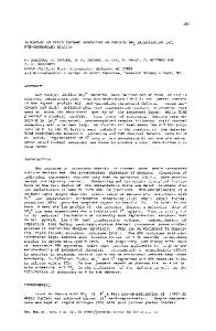
Thomas J. Watson Research Center, Yorktown Heights, NY **Eaton Ion Implantation Systems, 16 Tozer Road, Beverly, MA 01915 *IBM
10598;
ABSTRACT Silicon implanted with arsenic or boron has been annealed with a 100kW argon arc lamp turned on for a few seconds until the wafer temperature was in the 850-1250 0 C temperature range. The differences in defect behavior between such rapid annealing and furnace annealing is pointed out, and the dopant diffusion is measured. Aside from an initial movement of the boron atoms left in interstitial positions after the implant, diffusion of the boron and arsenic is consistent with standard diffusion models. Rapid thermal annealing has the advantage over normal furnace annealing of silicon that the wafer is relatively less time at "bad" temperatures of 600-800'C than at "good" temperatures of 1000-1200 0 C. Dopant segregation and growth and agglomeration of point defects and dislocations which are characteristic of the 600-800'C region can thus be reduced or avoided.
I
I
i
S
\
I
* 200C
550°C
oo
9o-c
90
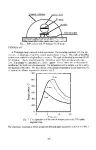
Fig. 1 Sketch of cross-sectional view of arsenic amorphized silicon as temperature is raised in normal furnace annealing (a) and rapid thermal annealing (b).
*
The dopant distribution is given
by the dashed line, and the amorphous region is the hatched area.
950C --T
Mat.
Res. Soc.
Symp. Proc. Vol.
_J.
23 (1984))Elsevier Science Publishing Co.,
Inc.
254
Figure 1 depicts the phenomena which occurs as the temperature is raised from room temperature in normal furnace annealing [1] (a) and rapid lamp annealing (b) for silicon implanted with sufficient arsenic ions so that the surface is amorphized. TEM analysis of the starting material shows a layer of small (~100A) interstitial dislocation loops lying "100A beneath the amorphous-crystal interface. As this material is heated past 550'C in a furnace, the crystal interface moves to the material surface with a well-defined rate [2] which depends on doping conditions, crystal orientation, and temperature. In furnace annealing, the small dislocation loops grow until they touch each other, then form two sets of larger loops with Burger's vectors parallel to the wafer plane. With continued heat treatment, the edge dislocation segments climb normal to the wafer surface and form half loops. Initially, the edge segments climb deeper into the crystal to depths of 100-200nm, but when the dopant front (as depicted by the dashed line in Fig. 1) passes them, they reverse direction, climb to the surface and disappear. In the meantime, the dopant front has moved an appreciable distance from its as implanted position. In contrast, the rapidly annealed silicon, Fig. lb, shows little growth of the original dislocation loops. At high temperatures (>1150' for 1 sec), the dopant front moves past them, and they disappear.
1020
-lOis
0 IiJ
tOIT
U I-
10 06
i015
1014 0
TIME (see) DEPTH(/Lm)
Fig. 2 SIMS curves for a series of
Data Loading...