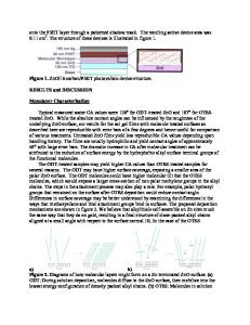
Improving the Efficiency of Organic Photovoltaic Devices through Interface Engineering
- PDF / 1,023,397 Bytes
- 6 Pages / 612 x 792 pts (letter) Page_size
- 18 Downloads / 535 Views
Improving the Efficiency of Organic Photovoltaic Devices through Interface Engineering Feilong Liu,1,2 Brian K. Crone,2 P. Paul Ruden,1,2 and Darryl L. Smith1,2 1 University of Minnesota, Minneapolis, MN 55455, U.S.A. 2 Los Alamos National Laboratory, Los Alamos, NM 87545, U.S.A. ABSTRACT We explore theoretically the effect of incorporating a thin tunnel barrier between the electron and hole transport layers of organic heterostructure photovoltaic devices. The device efficiency can be improved significantly by controlling the rates of microscopic processes associated with exciton dissociation and recombination at the interface between the electron and hole transport layers. The effects of different parameters are examined, and conclusions for organic photovoltaic device design are discussed. INTRODUCTION Organic semiconductor photovoltaic devices are promising for future energy conversion applications due to their low cost, ease of fabrication, and flexibility [1,2]. However, a major limitation of these devices is their low efficiency [3]. In order to improve the device efficiency various approaches have been explored, such as bulk heterojunction structures [4], blocking of exciton quenching [5], enhancement of charge collection [6], etc. The working principle of organic photovoltaic devices is based on the following processes. Excitons are generated by light absorption and subsequently dissociated at a heterojunction to form mobile electrons and holes. The generated electrons and holes flow to the corresponding contacts and a photocurrent is produced. A measure of device efficiency is the magnitude of the photocurrent under zero bias. Because of geminate processes [7,8], charge transfer states (or exciplexes) are usually formed shortly after the exciton dissociation. These excitations subsequently either relax to the ground state or dissociate into electrons and holes. The processes are summarized in figure 1.
Figure 1. Schematic of critical microscopic processes in organic photovoltaic devices. THEORY As shown in figure 1, in order to yield good device efficiency, (i) exciton dissociation (ED) should dominate over exciton recombination (ER), and (ii) charge transfer state
dissociation (CTD) should dominate over charge transfer state recombination (CTR). For typical devices where the interface of the heterojunction is designed to facilitate exciton dissociation, (i) is readily achieved. However, for the charge transfer states there is generally no guarantee that CTD will dominate over CTR, and hence (ii) may limit the overall efficiency. One option to improve the ratio of CTD to CTR is to insert a thin insulating layer between the electron transport layer (ETL) and the hole transport layer (HTL) [9]. For the charge transfer state, the bound electron and hole reside on the ETL and HTL molecules, respectively, separated by the insulating layer. The CTR rate depends on the wavefunction overlap between the bound electron and hole; as their separation increases with the insulating layer thickness, the CTR rate decrea
Data Loading...