In-situ early stage electromigration study in Al line using synchrotron polychromatic X-ray microdiffraction
- PDF / 406,824 Bytes
- 6 Pages / 612 x 792 pts (letter) Page_size
- 82 Downloads / 438 Views
1079-N05-02
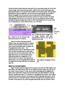
In-situ early stage electromigration study in Al line using synchrotron polychromatic X-ray microdiffraction Kai Chen1,2, N. Tamura1, and K. N. Tu2 1 Advanced Light Source, Lawrence Berkeley National Laboratory, 1 Cyclotron Road, Berkeley, CA, 94720 2 Department of Materials Science and Engineering, UCLA, Los Angeles, CA, 90095 ABSTRACT Electromigration is a phenomenon that has attracted much attention in the semiconductor industry because of its deleterious effects on electronic devices (such as interconnects) as they become smaller and current density passing through them increases. However, the effect of the electric current on the microstructure of interconnect lines during the very early stage of electromigration is not well documented. In the present report, we used synchrotron radiation based polychromatic X-ray microdiffraction for the in-situ study of the electromigration induced plasticity effects on individual grains of an Al (Cu) interconnect test structure. Dislocation slips which are activated by the electric current stressing are analyzed by the shape change of the diffraction peaks. The study shows polygonization of the grains due to the rearrangement of geometrically necessary dislocations (GND) in the direction of the current. Consequences of these findings are discussed. INTRODUCTION Electromigration (EM) refers to the mass transport phenomenon of materials due to electric current when the current density reaches high values. This phenomenon can have deleterious effects on microelectronic devices such as integrated circuits (ICs) [1]. In very-largescale integration (VLSI) of circuits on a Si device, Al or Cu thin-film line can experience current density as high as 106 A/cm2, which is enough to cause the atomic motion from the cathode end to the anode end at the device working temperature. Thus voids may form at the cathode end and extrusion may be squeezed out at the anode end, respectively [2]. Although a lot of models have been proposed to understand the mechanism of EM [3-6] , the effect of the atomic transport on the dislocation movement and local material microstructure, especially in the early stage of EM is still unclear. High brilliance X-ray beam with submicron to micron beam size can be produced by focusing optics such as Kirkpatrick-Baez (KB) mirrors at synchrotron facilities [7, 8]. X-ray microdiffraction has been developed for the crystal microstructure study. In this technique, since the crystal grains are larger than the X-ray beam size, a single crystal Laue diffraction pattern is obtained when polychromatic (white beam) X-ray impinges on the sample. By analyzing the Laue diffraction pattern, the orientation and strain information of the material irradiated can be obtained, and the spatial resolution is only limited by the size of the focused X-ray beam.
Previous works have shown the potential of Laue X-ray microdiffraction for EM study on interconnect lines [9-15]. In the present report, we report a more in-depth microstructure study in an Al (0.5 wt % Cu) interconn
Data Loading...