Electrochemical Etching in the GaN-Based Technology
- PDF / 2,335,614 Bytes
- 6 Pages / 414.72 x 648 pts Page_size
- 4 Downloads / 333 Views
513 Mat. Res. Soc. Symp. Proc. Vol. 512 01998 Materials Research Society
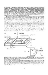
EXPERIMENT AND RESULTS Electrochemical etching was performed utilizing epilayers and structures grown by means of hydride vapor phase epitaxy (HVPE) and metalorganic chemical vapor deposition (MOCVD). Conductive GaN layers was selectively etched in the alkali electrolyte based on KOH or NaOH water solution (0.1-0.2 mol% ). The GaN-layer and Pt electrode were used as anode and cathode respectively. The electrical contact to GaN was masked from the electrolyte by a wax. Etching experiments were performed using a dc voltage (40-100 V) supply at room temperature and current density was in the range of 0,05-0,1 A/cm2 [4]. MOCVD-grown single GaN epilayers The GaN single epilayers with specular surfaces both undoped and doped with Si were grown in a conventional MOCVD system at a low pressure of 200 mbar. Ammonia and trimethylgallium were applied as component precursors. Purified hydrogen was used as a carrier gas. Silane was used for doping. The substrates were (0001) optical grade polished sapphire. The growth procedure included GaN nucleation layer deposition at a low temperature of 500 C followed by epilayers growth at a higher temperature of 1040 C The typical layer thickness under investigation was 2-4 ptm. The two-dimensional growth mode appeared to be dominant on the specular surfaces. Any hexagonal growth features were lacking, whereas the growth steps of -0.3 nm height were well defined by AFM. The only type of the surface defects were pinholes less than 0.5 gtm in diameter which were found on the surface of several samples while the others were featureless. Our investigations demonstrated that electrical properties of the undoped GaN epilayers grown by MOCVD were nonuniform. C-V measurements revealed that net donor concentration Nd-N. varied with epilayer depth. As shown in Fig. 1, the low concentration ranging from 5*10'5 cm 3 to 3*1016 cm 3 was observed to a depth of 1-1.55tgm whereas a rise of the concentration to 10107 cm"3 was measured as the depth increased. A f1
.A
A1203
Epilayer
substrate
surface
*
S&ooo
- this work, undoped GaN layer 13 - this work, Si-doped GaN layer * - data from ref. [5]
IE+18 1
1E+17, Z
1E+16
,7
z zmo
100Z-
lO
•
Nd-Na)
!1
E 1E+15 1
_____________
2
1
Depth, Am
V~)
0
10...
.......
IE+16
1E+17
IE+18
1E+19 IE+20
concentration , cm -3
Fig. I C-V profiling of undoped GaN layer
Fig.2 Comparison of Hall-effect and C-V measurements
514
For these layers, the Hall effect measurements gave the concentration of (1-5)* 1017 cm 3 and the mobility of 10-40 cm 2/V*s . Electron Hall mobility in relation to Nd-Na concentration along with published relationship between Hall mobility and electron concentration are plotted in Fig.2. Noticeable disagreement between C-V and Hall effect measurements could be related to a conductive channel present in the undoped GaN epilayer. In contrast, for Sidoped layers the results of C-V and Hall effect measurements were in close agreement. For example, the
Data Loading...