In-Situ Observation of UV/Ozone Oxidation of Silicon using Spectroscopic Eli Psometry
- PDF / 1,834,572 Bytes
- 6 Pages / 417.6 x 639 pts Page_size
- 11 Downloads / 227 Views
compositions non-destrucvely, but also to perform real-time data acquisition and analysis of the processing as well as to understand monolayer-level surface phenomena (5). Generally, ozone oxidation for silicon processes has been utilized to clean up the wafer surfaces by burning away organic contaminants In addition, the ozone process has been applied to prepare a very thin silicon oxide layer possibly for future silicon MOS devices. It was reported that the ozone oxidation was effective to realize enhanced oxidation at low temperatures (6,7) and to reduce a transition layer thickness at SiOz/Si interface (8). In this paper, initial process of silicon oxide growth in ozone ambient has been monitored using a multi-wavelength, in-situ ellipsometry. The oxide growth was examined as functions of wafer temperature, ozone pressure and time. The growth data %e discussed using an oxidation model with an electric field at the SiO2/Si interface. EXPERIMENT Silicon surfaces were oxidized in UV/ozone ambient using a vacutm growth chamber with in-situ spectroscopic ellipsometi. The chamber was equipped with two right and left-side ports for the in-situ SE measurement consisting of polarizer and analyzer with an inclined angle of 75 degrees. The in-situ setup (NM-44) supplied by J. A. Woollam Co. could measure 44 wavelengths from 280 to 600 rnm very fast using a silicon photodiode army and analyze the acquisition data using the sophisticated hardware and software (9). An average time for the data acquisition and analysis was less than 1 s for the 44 101
Mat. Res. Soc. Symp. Proc. Vol. 569 ©1999 Materials Research Society
wavelengths. Ulmviolet light wilh a 254-nm wavelength was illuminated from a low-pressure Hg lamp, 2 2 cm apart fiom the silicon surface. The intensity of the UV light was abou 20 mW/cm .Ozone gas was chemically formed by photochemical reaction of flowing-oxygen under the UV illuminaion. The temperature of the wafers was controlled up to 500C by a feedback mamer. The surface temperawte was monitored optically using the SE data and corrected using Si dielectric function data reported by Jellison. (10).
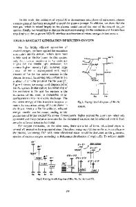
Proc Fig I
chamber
A UV/ozone oxidation chamber with in-situ spectroscopic ellipsometer.
RESULTS Determiatfion of ey-_Thin Oxide Thikm Very thin oxide thickness for the UV/ozomn and thermal oxides were determined using both spetroscopic ellipiometry (SE) and X-ray photoelectn sectroscopy (XPS). To assume a strctual model for the SE analysis, XPS was utilized The XPS analysis clarified that the quality of the UV/ozone oxide is almost close to that of hermal Si oxide prepared at a high temperature. Based on the result, it was assumed that the oxide sUucture consisted of thin thermal oxide layer and about 0.5-nm thick SiO2/Si mixture at the SiO2/Si interface. The dielectric function of the interface layer was calculated using a Bruggeman effective medium approximation. The thickness for both two layers was determined by obtaining a minimum mean-squarel error (MSE) between calculated and measured data TIe MSE w
Data Loading...