In Situ SEM Observations of Electromigration Voids in Al Lines under Passivation
- PDF / 2,754,743 Bytes
- 5 Pages / 576 x 792 pts Page_size
- 68 Downloads / 367 Views
tu SEM Observations of Electromigration Voids in Al Lines under Passivation Paul A. Flinn, Michael C. Madden, and Thomas N. Marieb Introduction Since the early work of Ilan Blech and Gene Meieran1 more than 20 years ago, electromigration (mass transport produced in a metallic conductor by current flow) has been recognized as an important reliability hazard for solid-state electronic devices. The continuing shrinkage of dimensions in VLSI devices has resulted in a continuing increase in the current density in the interconnection lines and a corresponding increase in the potential electromigration hazard. Although there have been improvements in the materials and structures used for interconnections, notably the addition of copper to aluminum and the use of layered structures, the provision of an adequate margin of safety has become increasingly difficult and is an important constraint on both device design and process development. A vast amount of effort has been expended over the years in attempts to characterize and understand electromigration failures and there is an extensive body of "conventional wisdom" on the subject. The basic physics of the process is well understood.2 The "electron wind" the momentum transfer from the scattering of conduction electrons by defects, produces a bias in the random walk of vacancies in the metal. An atom is more likely to jump into a vacant site if the jump is "downwind;' and less likely to jump "upwind" The result is a net flux of atoms in the direction of electron flow and a net flux of vacancies in the opposite direction. Any divergence in this flux will result in a local supersaturation of vacancies and the possibility of vacancy MRS BULLETIN/JUNE 1994
51
In Situ SEM Observations of Eiectromigration Voids in Al Lines under Passivation
vations were carried out, but on unpassivated metal. In 1984, Levine and Kitcher8 showed by optical microscopic observation that the behavior of voids and the mecha-
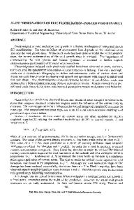
Figure 1. (a) Conventional image using secondary electrons; no void is visible, (b) Same sample with image from backscattered electrons; void is clearly seen through 0.7 y.m of passivation when using 120 kV accelerating voltage. '6
nism of eiectromigration failure are totally different when the metal is enclosed in dielectric. Instead of the conventional quasistatic picture of voids nucleating at triple points and growing in place to cause failure, they found that voids nucleate at sidewalls, travel large distances, and show very complicated behavior before failure occurs. Unfortunately, the use of optical microscopy had serious limitations. In addition to the poor resolution, only voids intersecting the interface between the top surface of the metal and the dielectric were visible. Also, it was necessary to interrupt the tests to carry out the measurements. In 1991, Castarb et al.9 showed that in situ SEM observation of void dynamics in metal lines under passivation was possible by using backscattered electron detection rather than the usual detection of secondary electrons.
Data Loading...